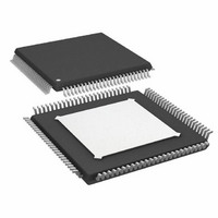
AD9445BSVZ-105 Analog Devices Inc, AD9445BSVZ-105 Datasheet - Page 3

AD9445BSVZ-105
Manufacturer Part Number
AD9445BSVZ-105
Description
IC,A/D CONVERTER,SINGLE,14-BIT,BICMOS,TQFP,100PIN
Manufacturer
Analog Devices Inc
Datasheet
1.AD9445BSVZ-105.pdf
(40 pages)
Specifications of AD9445BSVZ-105
Design Resources
Using AD8376 to Drive Wide Bandwidth ADCs for High IF AC-Coupled Appls (CN0002) Using AD8352 as an Ultralow Distortion Differential RF/IF Front End for High Speed ADCs (CN0046) Using ADL5562 Differential Amplifier to Drive Wide Bandwidth ADCs for High IF AC-Coupled Appls (CN0110)
Number Of Bits
14
Sampling Rate (per Second)
105M
Data Interface
Parallel
Number Of Converters
1
Power Dissipation (max)
2.4W
Voltage Supply Source
Single Supply
Operating Temperature
-40°C ~ 85°C
Mounting Type
Surface Mount
Package / Case
100-TQFP Exposed Pad
Lead Free Status / RoHS Status
Lead free / RoHS Compliant
Available stocks
Company
Part Number
Manufacturer
Quantity
Price
Company:
Part Number:
AD9445BSVZ-105
Manufacturer:
ADI
Quantity:
131
Company:
Part Number:
AD9445BSVZ-105
Manufacturer:
Analog Devices Inc
Quantity:
10 000
SPECIFICATIONS
DC SPECIFICATIONS
AVDD1 = 3.3 V, AVDD2 = 5.0 V, DRVDD = 3.3 V, LVDS mode, specified minimum sampling rate, 2.0 V p-p differential input, internal
trimmed reference (1.0 V mode), AIN = −1.0 dBFS, DCS on, unless otherwise noted. RF ENABLE = AGND.
Table 1.
Parameter
RESOLUTION
ACCURACY
VOLTAGE REFERENCE
INPUT REFERRED NOISE
ANALOG INPUT
POWER SUPPLIES
POWER CONSUMPTION
1
2
3
Measured at the maximum clock rate, f
approximately 5 pF loading on each output bit for CMOS output mode.
Input capacitance or resistance refers to the effective impedance between one differential input pin and AGND. Refer to Figure 6 for the equivalent analog input structure.
For RF ENABLE = AVDD1, I
No Missing Codes
Offset Error
Gain Error
Differential Nonlinearity (DNL)
Integral Nonlinearity (INL)
Output Voltage VREF = 1.0 V
Load Regulation @ 1.0 mA
Reference Input Current (External VREF = 1.6 V)
Input Span
Internal Input Common-Mode Voltage
External Input Common-Mode Voltage
Input Resistance
Input Capacitance
Supply Voltage
Supply Current
PSRR
LVDS Outputs
CMOS Outputs (DC Input)
VREF = 1.6 V
VREF = 1.0 V
AVDD1
AVDD2
DRVDD—LVDS Outputs
DRVDD—CMOS Outputs
AVDD1
AVDD2
I
I
Offset
Gain
DRVDD
DRVDD
1
1
—LVDS Outputs
—CMOS Outputs
1, 3
1
2
2
AVDD2
increases by ~30 mA, which increases power dissipation.
1
1
IN
= 15 MHz, full-scale sine wave, with a 100 Ω differential termination on each pair of output bits for LVDS output mode and
Temp
Full
Full
Full
25°C
Full
25°C
Full
25°C
Full
Full
Full
Full
25°C
Full
Full
Full
Full
Full
Full
Full
Full
Full
Full
Full
Full
Full
Full
Full
Full
Full
Full
Rev. 0 | Page 3 of 40
Min
−7
−3
−2
−0.6
5
−1.6
0.9
3.14
4.75
3.0
3.0
3.1
AD9445BSVZ-105
Guaranteed
Typ
14
±3
±0.25
±0.65
1.0
±2
1.0
3.2
2.0
3.5
1
6
3.3
5.0
3.3
335
169
63
14
1
0.2
2.2
2.0
Max
+7
+3
+2
+0.65
+1.6
1.1
3.9
3.46
5.25
3.6
3.6
364
196
78
2.4
Min
−7
−3
−2
−0.6
5
−2
0.9
3.1
3.14
4.75
3.0
3.0
AD9445BSVZ-125
Guaranteed
Typ
14
±3
±0.25
±0.8
1.0
±2
1.0
3.2
2.0
3.5
1
6
3.3
5.0
3.3
384
172
63
14
1
0.2
2.3
2.1
Max
+7
+3
+2
+0.65
+2
1.1
3.9
3.46
5.25
3.6
3.6
424
199
78
2.6
AD9445
Unit
Bits
mV
mV
% FSR
% FSR
LSB
LSB
LSB
V
mV
μA
LSB rms
V p-p
V p-p
V
V
kΩ
pF
V
V
V
V
mA
mA
mA
mA
mV/V
%/V
W
W


