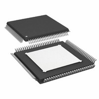
AD9445BSVZ-105 Analog Devices Inc, AD9445BSVZ-105 Datasheet - Page 6

AD9445BSVZ-105
Manufacturer Part Number
AD9445BSVZ-105
Description
IC,A/D CONVERTER,SINGLE,14-BIT,BICMOS,TQFP,100PIN
Manufacturer
Analog Devices Inc
Datasheet
1.AD9445BSVZ-105.pdf
(40 pages)
Specifications of AD9445BSVZ-105
Design Resources
Using AD8376 to Drive Wide Bandwidth ADCs for High IF AC-Coupled Appls (CN0002) Using AD8352 as an Ultralow Distortion Differential RF/IF Front End for High Speed ADCs (CN0046) Using ADL5562 Differential Amplifier to Drive Wide Bandwidth ADCs for High IF AC-Coupled Appls (CN0110)
Number Of Bits
14
Sampling Rate (per Second)
105M
Data Interface
Parallel
Number Of Converters
1
Power Dissipation (max)
2.4W
Voltage Supply Source
Single Supply
Operating Temperature
-40°C ~ 85°C
Mounting Type
Surface Mount
Package / Case
100-TQFP Exposed Pad
Lead Free Status / RoHS Status
Lead free / RoHS Compliant
Available stocks
Company
Part Number
Manufacturer
Quantity
Price
Company:
Part Number:
AD9445BSVZ-105
Manufacturer:
ADI
Quantity:
131
Company:
Part Number:
AD9445BSVZ-105
Manufacturer:
Analog Devices Inc
Quantity:
10 000
AD9445
DIGITAL SPECIFICATIONS
AVDD1 = 3.3 V, AVDD2 = 5.0 V, DRVDD = 3.3 V, R
Table 3.
Parameter
CMOS LOGIC INPUTS (DFS, DCS MODE, OUTPUT MODE)
DIGITAL OUTPUT BITS—CMOS MODE (D0 to D13, OTR)
DIGITAL OUTPUT BITS—LVDS MODE (D0 to D13, OTR)
CLOCK INPUTS (CLK+, CLK−)
1
2
SWITCHING SPECIFICATIONS
AVDD1 = 3.3 V, AVDD2 = 5.0 V, DRVDD = 3.3 V, unless otherwise noted.
Table 4.
Parameter
CLOCK INPUT PARAMETERS
DATA OUTPUT PARAMETERS
1
2
3
Output voltage levels measured with 5 pF load on each output.
LVDS R
With duty cycle stabilizer (DCS) enabled.
Output propagation delay is measured from clock 50% transition to data 50% transition with 5 pF load.
LVDS R
High Level Input Voltage
Low Level Input Voltage
High Level Input Current
Low Level Input Current
Input Capacitance
DRVDD = 3.3 V
V
V
Differential Input Voltage
Common-Mode Voltage
Differential Input Resistance
Differential Input Capacitance
Maximum Conversion Rate
Minimum Conversion Rate
CLK Period
CLK Pulse Width High
CLK Pulse Width Low
Output Propagation Delay—CMOS (t
Output Propagation Delay—LVDS (t
Pipeline Delay (Latency)
Aperture Delay (t
Aperture Uncertainty (Jitter, t
OD
OS
High Level Output Voltage
Low Level Output Voltage
Output Offset Voltage
Differential Output Voltage
TERM
TERM
= 100 Ω.
= 100 Ω. Measured from the 50% point of the rising edge of CLK+ to the 50% point of the data transition.
A
)
1
1
(t
(t
CLKL
CLKH
)
)
J
)
2
PD
PD
)
3
)
2
(Dx+), (t
(Dx, DCO+)
CPD
)
LVDS_BIAS
3
1
(DCO+)
= 3.74 kΩ, unless otherwise noted.
Rev. 0 | Page 6 of 40
Temp
Full
Full
Full
Full
Full
Full
Full
Full
Full
Full
Full
Full
Full
Temp
Full
Full
Full
Full
Full
Full
Full
Full
Full
Full
Min
2.0
−10
3.25
247
1.125
0.2
1.3
1.1
Min
105
9.5
3.8
3.8
2.1
AD9445BSVZ-105
AD9445BSVZ-105
Typ
3.35
3.6
13
60
Typ
2
1.5
1.4
2
Max
0.8
200
+10
0.2
545
1.375
1.6
1.7
Max
4.8
10
Min
125
8.0
3.2
3.2
2.3
Min
2.0
−10
3.25
247
1.125
0.2
1.3
1.1
AD9445BSVZ-125
AD9445BSVZ-125
Typ
3.35
3.6
13
60
Typ
2
1.5
1.4
2
Max
4.8
10
Max
0.8
200
+10
0.2
545
1.375
1.6
1.7
Unit
MSPS
MSPS
ns
ns
ns
ns
ns
Cycles
ns
fsec
rms
Unit
V
V
μA
μA
pF
V
V
mV
V
V
V
kΩ
pF


