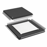
AD9445BSVZ-105 Analog Devices Inc, AD9445BSVZ-105 Datasheet - Page 29

AD9445BSVZ-105
Manufacturer Part Number
AD9445BSVZ-105
Description
IC,A/D CONVERTER,SINGLE,14-BIT,BICMOS,TQFP,100PIN
Manufacturer
Analog Devices Inc
Datasheet
1.AD9445BSVZ-105.pdf
(40 pages)
Specifications of AD9445BSVZ-105
Design Resources
Using AD8376 to Drive Wide Bandwidth ADCs for High IF AC-Coupled Appls (CN0002) Using AD8352 as an Ultralow Distortion Differential RF/IF Front End for High Speed ADCs (CN0046) Using ADL5562 Differential Amplifier to Drive Wide Bandwidth ADCs for High IF AC-Coupled Appls (CN0110)
Number Of Bits
14
Sampling Rate (per Second)
105M
Data Interface
Parallel
Number Of Converters
1
Power Dissipation (max)
2.4W
Voltage Supply Source
Single Supply
Operating Temperature
-40°C ~ 85°C
Mounting Type
Surface Mount
Package / Case
100-TQFP Exposed Pad
Lead Free Status / RoHS Status
Lead free / RoHS Compliant
Available stocks
Company
Part Number
Manufacturer
Quantity
Price
Company:
Part Number:
AD9445BSVZ-105
Manufacturer:
ADI
Quantity:
131
Company:
Part Number:
AD9445BSVZ-105
Manufacturer:
Analog Devices Inc
Quantity:
10 000
EVALUATION BOARD
Evaluation boards are offered to configure the AD9445 in
either CMOS or LVDS mode only. This design represents a
recommended configuration for using the device over a wide
range of sampling rates and analog input frequencies. These
evaluation boards provide all the support circuitry required to
operate the ADC in its various modes and configurations.
Complete schematics are shown in Figure 67 through Figure 70.
Gerber files are available from engineering applications demon-
strating the proper routing and grounding techniques that should
be applied at the system level.
It is critical that signal sources with very low phase noise
(<60 fsec rms jitter) be used to realize the ultimate performance
of the converter. Proper filtering of the input signal to remove
harmonics and lower the integrated noise at the input is also
necessary to achieve the specified noise performance.
The evaluation boards are shipped with a 115 V ac to 6 V dc
power supply. The evaluation boards include low dropout
regulators to generate the various dc supplies required by the
AD9445 and its support circuitry. Separate power supplies are
provided to isolate the DUT from the support circuitry. Each
input configuration can be selected by proper connection of
various jumpers (see Figure 67).
Rev. 0 | Page 29 of 40
The LVDS mode evaluation boards include an LVDS-to-CMOS
translator, making them compatible with the high speed ADC
FIFO evaluation kit (HSC-ADC-EVALA-SC). The kit includes a
high speed data capture board that provides a hardware solution
for capturing up to 32 kB samples of high speed ADC output
data in a FIFO memory chip (user upgradeable to 256 kB
samples). Software is provided to enable the user to download
the captured data to a PC via the USB port. This software also
includes a behavioral model of the AD9445 and many other
high speed ADCs.
Behavioral modeling of the AD9445 is also available at
www.analog.com/ADIsimADC. The ADIsimADC™ software
supports virtual ADC evaluation using ADI proprietary behavioral
modeling technology. This allows rapid comparison between
the AD9445 and other high speed ADCs with or without
hardware evaluation boards.
The user can choose to remove the translator and terminations
to access the LVDS outputs directly.
AD9445


