ADAU1445YSVZ-3A-RL Analog Devices Inc, ADAU1445YSVZ-3A-RL Datasheet - Page 13
ADAU1445YSVZ-3A-RL
Manufacturer Part Number
ADAU1445YSVZ-3A-RL
Description
175MHZ SigmaDSP,2x8 SRCs
Manufacturer
Analog Devices Inc
Series
SigmaDSP®r
Type
Audio Processorr
Specifications of ADAU1445YSVZ-3A-RL
Applications
Automotive Audio
Mounting Type
Surface Mount
Package / Case
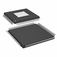
100-TQFP Exposed Pad, 100-eTQFP, 100-HTQFP, 100-VQFP
Format
Fixed Point
Program Memory Size
Not RequiredKB
Operating Supply Voltage (typ)
1.8/3.3V
Operating Temp Range
-40C to 105C
Operating Temperature Classification
Industrial
Mounting
Surface Mount
Pin Count
100
Lead Free Status / RoHS Status
Lead free / RoHS Compliant
Lead Free Status / RoHS Status
Lead free / RoHS Compliant
Available stocks
Company
Part Number
Manufacturer
Quantity
Price
Company:

Part Number:
ADAU1445YSVZ-3A-RL
Manufacturer:
Analog Devices Inc
Quantity:
10 000


Pin No.
6
7
8
9
10
11
12
15
16
17
18
19
20
21
22
23
24
25, 37,
50, 75,
87, 100
28
29
30
31
32
33
Mnemonic
BCLK2
LRCLK2
SDATA_IN1
BCLK1
LRCLK1
SDATA_IN0
BCLK0
LRCLK0
MP11
MP10
MP9
MP8
ADDR0
CLATCH
SCL/CCLK
SDA/COUT
ADDR1/CDATA
DVDD
SELFBOOT
CLKMODE1
CLKMODE0
RSVD
PLL2
MP7
Type
D_IO
D_IO
D_IN
D_IO
D_IO
D_IN
D_IO
D_IO
D_IO
D_IO
D_IO
D_IO
D_IN
D_IN
D_IN
D_IO
D_IN
PWR
D_IN
D_IN
D_IN
D_IN
D_IN
D_IO
1
Description
Bit Clock, Input Clock Domain 2. This pin is bidirectional, with the direction depending on whether
the Input Clock Domain 2 is set up as a master or slave. When not used, this pin can be left disconnected.
Frame Clock, Input Clock Domain 2. This pin is bidirectional, with the direction depending on whether
the Input Clock Domain 2 is set up as a master or slave. When not used, this pin can be left disconnected.
Serial Data Port 1 Input. When not used, this pin can be left disconnected.
Bit Clock, Input Clock Domain 1. This pin is bidirectional, with the direction depending on whether
the Input Clock Domain 1 is set up as a master or slave. When not used, this pin can be left disconnected.
Frame Clock, Input Clock Domain 1. This pin is bidirectional, with the direction depending on whether
the Input Clock Domain 1 is set up as a master or slave. When not used, this pin can be left disconnected.
Serial Data Port 0 Input. When not used, this pin can be left disconnected.
Bit Clock, Input Clock Domain 0. This pin is bidirectional, with the direction depending on whether
the Input Clock Domain 0 is set up as a master or slave. When not used, this pin can be left disconnected.
Frame Clock, Input Clock Domain 0. This pin is bidirectional, with the direction depending on whether
the Input Clock Domain 0 is set up as a master or slave. When not used, this pin can be left disconnected.
Multipurpose, General-Purpose Input/Output. When not used, this pin can be left disconnected.
Multipurpose, General-Purpose Input/Output. When not used, this pin can be left disconnected.
Multipurpose, General-Purpose Input/Output. When not used, this pin can be left disconnected.
Multipurpose, General-Purpose Input/Output. When not used, this pin can be left disconnected.
Address 0 for I
ADAU1442/ADAU1445/ADAU1446 devices to be used on the same I
ADDR0 either low or high allows up to two ICs to be used with a common SPI latch signal.
SPI Latch Signal. Must go low at the beginning of an SPI transaction and high at the end of a
transaction. Each SPI transaction may take a different number of CCLK cycles to complete,
depending on the address and read/write bits that are sent at the beginning of the SPI transaction.
When not used, this pin should be tied to ground, preferably with a 10 kΩ pull-down resistor.
Serial Clock/Continuous Clock. In I
input, except when in self-boot mode, where it is an open collector output (I
connected to this pin should have a 2.0 kΩ pull-up resistor. In SPI mode, this pin functions as CCLK
and is an input pin that can be either run continuously or gated off between SPI transactions.
Serial Data/Continuous Output. In I
collector. The line connected to the SDA pin should have a 2.0 kΩ pull-up resistor. In SPI mode, this
pin functions as COUT and is used for reading back registers and memory locations. The COUT pin
is three-stated when an SPI read is not active.
Address 1/Continuous Data. In I
ADDR0, sets the I
devices to be used on the same I
data input.
1.8 V Digital Supply. This can be supplied externally or generated from a 3.3 V supply with the on-board
1.8 V regulator. Each DVDD pin should be decoupled to DGND with a 100 nF capacitor.
Self-Boot Select. Allows the ADAU1442/ADAU1445/ADAU1446 to be controlled by the control port
or to perform a self-boot. Setting this pin high (that is, to 1) initiates a self-boot operation when the
ADAU1442/ADAU1445/ADAU1446 are brought out of a reset. This pin can be tied directly to a
voltage source or ground or pulled up/down with a resistor.
Output Clock Mode 1. With CLKMODE0, this pin sets the frequency of the CLKOUT signal.
Output Clock Mode 0. With CLKMODE1, this pin sets the frequency of the CLKOUT signal.
Reserved. Tie this pin to ground, preferably with a 10 kΩ pull-down resistor.
PLL Mode Select Pin 2.
Multipurpose, General-Purpose Input/Output. When not used, this pin can be left disconnected.
2
C and SPI. In I
2
C address of the IC. This allows up to four ADAU1442/ADAU1445/ADAU1446
Rev. C | Page 13 of 92
2
C mode, this pin, in combination with ADDR1, allows up to four
2
C mode, this pin functions as ADDR1 and, in combination with
2
2
C bus. In SPI mode, this pin functions as CDATA and is the SPI
C mode, this pin functions as SCL and is always an open collector
2
C mode, this pin functions as SDA and is a bidirectional open
ADAU1442/ADAU1445/ADAU1446
2
C bus. In SPI mode, setting
2
C master). The line
Related parts for ADAU1445YSVZ-3A-RL
Image
Part Number
Description
Manufacturer
Datasheet
Request
R

Part Number:
Description:
SigmaDSP� Digital Audio Processor with Flexible Audio Routing Matrix
Manufacturer:
Analog Devices
Datasheet:

Part Number:
Description:
±1.7g Dual-Axis IMEMS Accelerometer Evaluation Board
Manufacturer:
Analog Devices Inc
Datasheet:

Part Number:
Description:
Inertial Sensor Evaluation System
Manufacturer:
Analog Devices Inc
Datasheet:
Part Number:
Description:
Manufacturer:
Analog Devices Inc
Datasheet:
Part Number:
Description:
Manufacturer:
Analog Devices Inc
Datasheet:
Part Number:
Description:
Manufacturer:
Analog Devices Inc
Datasheet:
Part Number:
Description:
Manufacturer:
Analog Devices Inc
Datasheet:
Part Number:
Description:
Manufacturer:
Analog Devices Inc
Datasheet:
Part Number:
Description:
Manufacturer:
Analog Devices Inc
Datasheet:
Part Number:
Description:
Manufacturer:
Analog Devices Inc
Datasheet:
Part Number:
Description:
Manufacturer:
Analog Devices Inc
Datasheet:
Part Number:
Description:
Manufacturer:
Analog Devices Inc
Datasheet:
Part Number:
Description:
Manufacturer:
Analog Devices Inc
Datasheet: