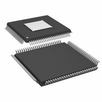
ADAU1445YSVZ-3A-RL Analog Devices Inc, ADAU1445YSVZ-3A-RL Datasheet - Page 30

ADAU1445YSVZ-3A-RL
Manufacturer Part Number
ADAU1445YSVZ-3A-RL
Description
175MHZ SigmaDSP,2x8 SRCs
Manufacturer
Analog Devices Inc
Series
SigmaDSP®r
Type
Audio Processorr
Specifications of ADAU1445YSVZ-3A-RL
Applications
Automotive Audio
Mounting Type
Surface Mount
Package / Case
100-TQFP Exposed Pad, 100-eTQFP, 100-HTQFP, 100-VQFP
Format
Fixed Point
Program Memory Size
Not RequiredKB
Operating Supply Voltage (typ)
1.8/3.3V
Operating Temp Range
-40C to 105C
Operating Temperature Classification
Industrial
Mounting
Surface Mount
Pin Count
100
Lead Free Status / RoHS Status
Lead free / RoHS Compliant
Lead Free Status / RoHS Status
Lead free / RoHS Compliant
Available stocks
Company
Part Number
Manufacturer
Quantity
Price
Company:
Part Number:
ADAU1445YSVZ-3A-RL
Manufacturer:
Analog Devices Inc
Quantity:
10 000
ADAU1442/ADAU1445/ADAU1446
Self-Boot
On power-up, the ADAU1442/ADAU1445/ADAU1446 can
load a program and a set of parameters that are saved in an
external EEPROM. Combined with the auxiliary ADC and the
multipurpose pins, this can potentially eliminate the need for a
microcontroller in a simple audio system. The self-boot sequence
is accomplished by the ADAU1442/ADAU1445/ADAU1446
acting as masters on the I
the SELFBOOT pin is set high. The ADAU1442/ADAU1445/
ADAU1446 cannot self-boot in SPI mode.
The maximum necessary EEPROM size is 40,960 bytes, or
40 kB. This much memory is only needed if the program RAM
(4096 × 6 bytes) and parameter RAM (4096 × 4 bytes) are each
completely full.
A self-boot operation is triggered on the rising edge of RESET
when the SELFBOOT pin is set high, and it occurs after 10 ms
when the PLL has locked. The ADAU1442/ADAU1445/
ADAU1446 read the program, parameter, and register data
from the EEPROM. After the ADAU1442/ADAU1445/ADAU1446
have finished self-booting, additional messages can be sent to the
ADAU1442/ADAU1445/ADAU1446 on the I
this typically is not necessary in a self-booting application. The
I
0x68 for a write and 0x69 for a read in this mode. The ADDRx pins
have different functions when the chip is in this mode; therefore,
the settings on them are ignored.
The ADAU1442/ADAU1445/ADAU1446 are masters on the I
bus during a self-boot operation. Care should be taken that no
Table 16. Functions of the Control Port Pins
Pin
SCL/CCLK
SDA/COUT
ADDR1/CDATA
CLATCH
ADDR0
Table 17. EEPROM Message Types
Message ID
0x00
0x01
0x02
0x03
2
C device address for the ADAU1442/ADAU1445/ADAU1446 is
2
C bus on startup, which occurs when
I
SCL—input
SDA—open collector output
ADDR1—input
Unused input—tie to ground or power
ADDR0—input
2
C Mode
Message Type
End
Write
Delay
No op
2
C bus, although
Rev. C | Page 30 of 92
2
C
SPI Mode
CCLK—input
COUT—output
CDATA—input
CLATCH—input
ADDR0—input
other device on the I
during self-booting. The ADAU1442/ADAU1445/ADAU1446
generate SCL at 8 × f
runs at 384 kHz. SCL has a duty cycle of ⅜ in accordance with
the I
The ADAU1442/ADAU1445/ADAU1446 read from EEPROM
Chip Address 0xA1. The LSBs of the addresses of some EEPROMs
are pin configurable; in most cases, these pins should be tied
low to set this address. SigmaStudio writes to the EEPROM at
Address 0xA0.
EEPROM Format
The EEPROM data contains a sequence of messages. Each
discrete message is one of the four types defined in Table 17.
Each message consists of a sequence of one or more bytes. The
first byte identifies the message type. Bytes are written MSB
first. Most messages are block write (0x01) types, which are
used for writing to the ADAU1442/ADAU1445/ADAU1446
program RAM, parameter RAM, and control registers.
The body of the message following the message type should
start with two bytes indicating message length and then include
a byte indicating the chip address. Following this is always a
2-byte register or memory address field, as with all other
control port transactions.
SigmaStudio is capable of generating the EEPROM data necessary
to self-boot the ADAU1442/ADAU1445/ADAU1446, using the
function called write latest compilation to E2PROM. This function
can be accessed by right-clicking the ADAU1442/ADAU1445/
ADAU1446 IC in the hardware configuration window.
Following Bytes
None
One byte indicating message length (including chip address and
subaddress), one byte indicating chip address, two bytes
indicating subaddress, and an appropriate number of data bytes
Two bytes for delay
None
2
C specification.
Self-Boot
SCL—output
SDA—open collector output
Unused input—tie to ground or power
Unused input—tie to ground or power
Unused input—tie to ground or power
2
s
C bus tries to perform a write operation
; therefore, when f
s,NORMAL
is 48 kHz, SCL


