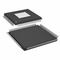
ADAU1445YSVZ-3A-RL Analog Devices Inc, ADAU1445YSVZ-3A-RL Datasheet - Page 65

ADAU1445YSVZ-3A-RL
Manufacturer Part Number
ADAU1445YSVZ-3A-RL
Description
175MHZ SigmaDSP,2x8 SRCs
Manufacturer
Analog Devices Inc
Series
SigmaDSP®r
Type
Audio Processorr
Specifications of ADAU1445YSVZ-3A-RL
Applications
Automotive Audio
Mounting Type
Surface Mount
Package / Case
100-TQFP Exposed Pad, 100-eTQFP, 100-HTQFP, 100-VQFP
Format
Fixed Point
Program Memory Size
Not RequiredKB
Operating Supply Voltage (typ)
1.8/3.3V
Operating Temp Range
-40C to 105C
Operating Temperature Classification
Industrial
Mounting
Surface Mount
Pin Count
100
Lead Free Status / RoHS Status
Lead free / RoHS Compliant
Lead Free Status / RoHS Status
Lead free / RoHS Compliant
Available stocks
Company
Part Number
Manufacturer
Quantity
Price
Company:
Part Number:
ADAU1445YSVZ-3A-RL
Manufacturer:
Analog Devices Inc
Quantity:
10 000
S/PDIF RECEIVER AND TRANSMITTER
The ADAU1442/ADAU1445/ADAU1446 each feature a set of
on-chip S/PDIF data ports, which can be wired directly to
transmitters and receivers for easy interfacing to other S/PDIF-
compatible equipment.
S/PDIF Receiver
The S/PDIF input port is designed to accept both TTL and
bipolar signals, provided there is an ac coupling capacitor on
the input pin of the chip. Because the S/PDIF input data will
most likely be asynchronous to the DSP core, it must be routed
through an ASRC.
The S/PDIF ports work with sampling rates between 32 kHz
and 108 kHz.
In addition to audio data, S/PDIF streams contain user data,
channel status, validity bit, virtual LRCLK, and block start
information. The receiver decodes audio data and sends it to
the ASRCs and DSP core, but the remaining data passes through
directly to the transmitter. This ensures that any user data is
unaltered at the output and is reintegrated into the audio stream.
In the ADAU1442/ADAU1445/ADAU1446, clock recovery
is entirely digital. As a result, the ADAU1442/ADAU1445/
ADAU1446 have better protection against clock jitter.
The ADAU1442/ADAU1445/ADAU1446 S/PDIF ports are
designed to meet the following AES and EBU specifications: a
jitter of 0.25 UI p-p at 8 kHz and above, a jitter of 10 UI p-p
below 200 Hz, and a minimum signal voltage of 200 mV.
To transmit data, the S/PDIF output must be turned on. This is
accomplished by writing an activation bit to the S/PDIF transmitter
on/off register. More information can be found in the Enable
SPDIFI
RECEIVER
S/PDIF
Figure 53. S/PDIF Receiver and Transmitter
AUDIO
AUDIO
DATA
AND
Rev. C | Page 65 of 92
CONVERTER
DSP CORE
ASRCs
I
2
S
S/PDIF to I
On/Off Switch Register (Address 0xE0C1) section.
Outputting to the Multipurpose Pins
It is possible to send S/PDIF data from the receiver directly to
output on the MP pins. This mode is activated in Register 0xE241
(see the Enable S/PDIF to I
assignment of signals is shown in Table 53.
Table 53. S/PDIF to MP Pin Assignments
Pin
MP4
MP5
MP6
MP7
MP8
MP9
MP10
MP11
1
There are two groups of signals, each of which can be activated
and deactivated independent from one another. All unused MP
pins function normally.
S/PDIF Transmitter
The S/PDIF transmitter outputs two channels of audio data
directly from the DSP core at the core rate. It does not preserve
or output any additional nonaudio information encoded in the
S/PDIF input stream. The encoded nonaudio data bits in the
S/PDIF stream are low, except for the validity bit, which is high.
Some S/PDIF receivers will ignore the transmitted audio data
because the high validity bit indicates an error.
The MP0 to MP3 pins are not applicable and can be used normally.
MP PINS
1
5
TRANSMITTER
BCLK
LRCLK
SDATA
DATA BITS
S/PDIF
2
S Output section and the S/PDIF Transmitter—
ADAU1442/ADAU1445/ADAU1446
Group
2
2
2
2
2
1
1
1
MASTER
MODE
SPDIFO
2
S Output section). The pin
Signal
Validity bit
User data
Channel select
Block start
Virtual LRCLK
SDATA
BCLK
LRCLK


