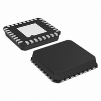
ADUC7061BCPZ32-RL Analog Devices Inc, ADUC7061BCPZ32-RL Datasheet - Page 15

ADUC7061BCPZ32-RL
Manufacturer Part Number
ADUC7061BCPZ32-RL
Description
DUAL 24-BIT AFE AND ARM 7 I.C
Manufacturer
Analog Devices Inc
Series
MicroConverter® ADuC7xxxr
Datasheet
1.EVAL-ADUC7061MKZ.pdf
(108 pages)
Specifications of ADUC7061BCPZ32-RL
Design Resources
USB Based Temperature Monitor Using ADuC7061 and an External RTD (CN0075) 4 mA-to-20 mA Loop-Powered Temperature Monitor Using ADuC7060/1 (CN0145)
Core Processor
ARM7
Core Size
16/32-Bit
Speed
10MHz
Connectivity
I²C, SPI, UART/USART
Peripherals
POR, PWM, Temp Sensor, WDT
Number Of I /o
8
Program Memory Size
32KB (32K x 8)
Program Memory Type
FLASH
Ram Size
4K x 8
Voltage - Supply (vcc/vdd)
2.375 V ~ 2.625 V
Data Converters
A/D 5x24b, 8x24b, D/A 1x14b
Oscillator Type
Internal
Operating Temperature
-40°C ~ 125°C
Package / Case
32-LFCSP
Lead Free Status / RoHS Status
Lead free / RoHS Compliant
Eeprom Size
-
Lead Free Status / RoHS Status
Lead free / RoHS Compliant
PIN CONFIGURATIONS AND FUNCTION DESCRIPTIONS
Table 8. ADuC7060 Pin Function Descriptions
Pin
No.
0
1
2
3
4
5
6
7
8
9
10
11
Mnemonic
EP
RESET
TMS
P1.0/IRQ1/SIN/T0
P1.1/SOUT
P1.2/SYNC
P1.3/TRIP
P0.5/CTS
P0.6/RTS
DVDD
DGND
DAC0
ADC5/EXT_REF2IN−
NOTES
1. THE LFCSP_VQ ONLY HAS AN EXPOSED PADDLE THAT MUST BE LEFT UNCONNECTED.
THIS DOES NOT APPLY TO THE LQFP.
Type
I
I
I/O
I/O
I/O
I/O
I/O
I/O
S
S
O
P1.0/IRQ1/SIN/T0
P1.1/SOUT
P1.2/SYNC
1
P1.3/TRIP
P0.5/CTS
P0.6/RTS
Figure 7. 48-Lead LQFP and 48-Lead LFCSP_VQ Pin Configuration
RESET
DGND
DVDD
DAC0
Description
Exposed Paddle. The LFCSP_VQ only has an exposed paddle that must be left unconnected.
This does not apply to the LQFP.
Reset. Input pin, active low. An external 1 kΩ pull-up resistor is recommended with this pin.
JTAG Test Mode Select. Input pin used for debug and download. An external pull-up resistor
(~100 kΩ) should be added to this pin.
General-Purpose Input and General Purpose Output P1.0/External Interrupt Request 1/Serial
Input/Timer0 Input. This is a multifunction input/output pin offering four functions.
General-Purpose Input and General-Purpose Output P1.1/Serial Output. This is a dual function
input/output pin.
General-Purpose Input and General-Purpose Output P1.2/PWM External Sync Input. This is a
dual function input/output pin.
General-Purpose Input and General-Purpose Output P1.3/PWM External Trip Input. This is a
dual function input/output pin.
General-Purpose Input and General-Purpose Output P0.5/Clear-to-Send Signal in UART Mode.
General-Purpose Input and General-Purpose Output P0.6/Request-to-Send Signal in UART Mode.
Digital Supply Pin.
Digital Ground.
DAC Output. Analog output pin.
TMS
10
11
12
1
2
3
4
5
6
7
8
9
PIN 1
INDICATOR
Rev. B | Page 15 of 108
ADuC7060
(Not to Scale)
TOP VIEW
36
35
34
33
32
31
30
29
28
27
26
25
XTALI
XTALO
P0.3/MOSI/SDA
P0.2/MISO
P0.1/SCLK/SCL
P0.0/SS
DVDD
DGND
ADC9
ADC8
ADC7
ADC6
ADuC7060/ADuC7061


