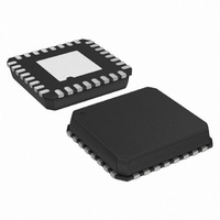
ADUC7061BCPZ32-RL Analog Devices Inc, ADUC7061BCPZ32-RL Datasheet - Page 50

ADUC7061BCPZ32-RL
Manufacturer Part Number
ADUC7061BCPZ32-RL
Description
DUAL 24-BIT AFE AND ARM 7 I.C
Manufacturer
Analog Devices Inc
Series
MicroConverter® ADuC7xxxr
Datasheet
1.EVAL-ADUC7061MKZ.pdf
(108 pages)
Specifications of ADUC7061BCPZ32-RL
Design Resources
USB Based Temperature Monitor Using ADuC7061 and an External RTD (CN0075) 4 mA-to-20 mA Loop-Powered Temperature Monitor Using ADuC7060/1 (CN0145)
Core Processor
ARM7
Core Size
16/32-Bit
Speed
10MHz
Connectivity
I²C, SPI, UART/USART
Peripherals
POR, PWM, Temp Sensor, WDT
Number Of I /o
8
Program Memory Size
32KB (32K x 8)
Program Memory Type
FLASH
Ram Size
4K x 8
Voltage - Supply (vcc/vdd)
2.375 V ~ 2.625 V
Data Converters
A/D 5x24b, 8x24b, D/A 1x14b
Oscillator Type
Internal
Operating Temperature
-40°C ~ 125°C
Package / Case
32-LFCSP
Lead Free Status / RoHS Status
Lead free / RoHS Compliant
Eeprom Size
-
Lead Free Status / RoHS Status
Lead free / RoHS Compliant
ADuC7060/ADuC7061
Table 52. ADC1OF MMR Bit Designations
Bit
15:0
Primary Channel ADC Gain Calibration Register
Name:
Address:
Default value:
Access:
Function:
Table 53. ADC0GN MMR Bit Designations
Bits
15:0
Auxiliary Channel Gain Calibration Register
Name:
Address:
Default value:
Access:
Function:
Table 54. ADC1GN MMR Bit Designations
Bits
15:0
Description
ADC1 16-bit offset calibration value.
ADC0GN
0xFFFF052C
Part specific, factory programmed
Read and write
This gain MMR holds a 16-bit gain
calibration coefficient for scaling the primary
ADC conversion result. The register is
configured at power-on with a factory default
value. However, this register is automatically
overwritten if a gain calibration of the
primary ADC is initiated by the user via bits
in the ADCMDE MMR. User code can write
to this calibration register only if the ADC is
in idle mode. An ADC must be enabled and
in idle mode before being written to any
offset or gain register. The ADC must be in
idle mode for at least 23 μs.
Description
ADC0 16-bit calibration gain value.
ADC1GN
0xFFFF0530
Part specific, factory programmed
Read and write
This gain MMR holds a 16-bit gain calibra-
tion coefficient for scaling an auxiliary channel
conversion result. The register is configured
at power-on with a factory default value.
However, this register is automatically over-
written if a gain calibration of the auxiliary
channel is initiated by the user via bits in the
ADCMDE MMR. User code can write to this
calibration register only if the ADC is in idle
mode. An ADC must be enabled and in idle
mode before being written to any offset or gain
register. The ADC must be in idle mode for at
least 23 μs.
Description
ADC1 16-bit gain calibration value.
Rev. B | Page 50 of 108
Primary Channel ADC Result Counter Limit Register
Name:
Address:
Default value:
Access:
Function:
Table 55. ADC0RCR MMR Bit Designations
Bits
15:0
Primary Channel ADC Result Counter Register
Name:
Address:
Default value:
Access:
Function:
Table 56. ADC0RCV MMR Bit Designations
Bits
15:0
ADC0RCR
0xFFFF0534
0x0001
Read and write
This 16-bit MMR sets the number of
conversions required before an ADC
interrupt is generated. By default, this
register is set to 0x01. The ADC counter
function must be enabled via the ADC result
counter enable bit in the ADCCFG MMR.
Description
ADC0 result counter limit/reload register.
ADC0RCV
0xFFFF0538
0x0000
Read only
This 16-bit, read-only MMR holds the
current number of primary ADC conversion
results. It is used in conjunction with
ADC0RCR to mask primary channel ADC
interrupts, generating a lower interrupt rate.
When ADC0RCV = ADC0RCR, the value in
ADC0RCV resets to 0 and recommences
counting. It can also be used in conjunction
with the accumulator (ADC0ACC) to allow
an average calculation to be taken. The
result counter is enabled via ADCCFG[0].
This MMR is also reset to 0 when the
primary ADC is reconfigured, that is, when
the ADC0CON or ADCMDE is written.
Description
ADC0 result counter register.


