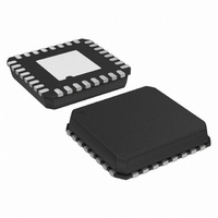
ADUC7061BCPZ32-RL Analog Devices Inc, ADUC7061BCPZ32-RL Datasheet - Page 33

ADUC7061BCPZ32-RL
Manufacturer Part Number
ADUC7061BCPZ32-RL
Description
DUAL 24-BIT AFE AND ARM 7 I.C
Manufacturer
Analog Devices Inc
Series
MicroConverter® ADuC7xxxr
Datasheet
1.EVAL-ADUC7061MKZ.pdf
(108 pages)
Specifications of ADUC7061BCPZ32-RL
Design Resources
USB Based Temperature Monitor Using ADuC7061 and an External RTD (CN0075) 4 mA-to-20 mA Loop-Powered Temperature Monitor Using ADuC7060/1 (CN0145)
Core Processor
ARM7
Core Size
16/32-Bit
Speed
10MHz
Connectivity
I²C, SPI, UART/USART
Peripherals
POR, PWM, Temp Sensor, WDT
Number Of I /o
8
Program Memory Size
32KB (32K x 8)
Program Memory Type
FLASH
Ram Size
4K x 8
Voltage - Supply (vcc/vdd)
2.375 V ~ 2.625 V
Data Converters
A/D 5x24b, 8x24b, D/A 1x14b
Oscillator Type
Internal
Operating Temperature
-40°C ~ 125°C
Package / Case
32-LFCSP
Lead Free Status / RoHS Status
Lead free / RoHS Compliant
Eeprom Size
-
Lead Free Status / RoHS Status
Lead free / RoHS Compliant
OSCILLATOR, PLL, AND POWER CONTROL
CLOCKING SYSTEM
The ADuC706x integrates a 32.768 kHz ±3% oscillator, a clock
divider, and a PLL. The PLL locks onto a multiple of the inter-
nal oscillator or an external 32.768 kHz crystal to provide a stable
10.24 MHz clock (UCLK) for the system. To allow power saving,
the core can operate at this frequency or at binary submultiples
of it. The actual core operating frequency, UCLK/2
to as HCLK. The default core clock is the PLL clock divided by 8
(CD = 3) or 1.28 MHz.
External Crystal Selection
To switch to an external crystal, users must follow this procedure:
1.
2.
3.
4.
Example source code
T1LD
T1CON = 0xC0; // Periodic mode, enable
IRQEN |= 0x10; // Enable Timer1 interrupt
PLLKEY1 = 0xAA;
PLLCON = 0x2;
PLLKEY2 = 0x55;
POWKEY1 = 0x1;
POWCON0 = 0x73;
POWKEY2 = 0xF4;
*32.768kHz
WATCHDOG
WAKE-UP
TIMER
TIMER
Enable the Timer1 interrupt and configure it for a timeout
period of >120 μs.
Follow the write sequence to the PLLCON register, setting the
OSEL bits to [10] and clearing the EXTCLK bit.
Force the part into nap mode by following the correct write
sequence to the POWCON register.
When the part is interrupted from nap mode by the Timer1
interrupt source, the clock source has switched to the external
crystal.
= 0x80; // 32,768 clock ticks
±
3%
CORE
// source
// timer, 32,768 Hz clock/1
OSCILLATOR*
Figure 13. Clocking System
INT. 32kHz
// Switch to external crystal
// Enter nap mode
PLL
I
2
CD
C
32.768kHz
10.24MHz
UCLK
OCLK
/2
CD
HCLK
OSCILLATOR
CRYSTAL
PERIPHERALS
ANALOG
CD
, is refered
XCLKO
XCLKI
P2.0/EXTCLK
Rev. B | Page 33 of 108
In case of crystal loss, the watchdog timer should be used. During
initialization, a test on the RSTSTA can determine if the reset came
from the watchdog timer.
External Clock Selection
To switch to an external clock on P2.0, configure P2.0 in Mode 0.
The external clock can be up to 20.48 MHz, provided that the toler-
ance is 1%. The external clock is divided by 2 internally on the part.
Example source code
T1LD
T1CON = 0xC0;
IRQEN |= 0x10;
PLLKEY1 = 0xAA;
PLLCON = 0x4;
PLLKEY2 = 0x55;
POWKEY1 = 0x1;
POWCON0 = 0x73;
POWKEY2 = 0xF4;
The selection of the clock source is in the PLLCON register. By
default, the part uses the internal oscillator feeding the PLL.
POWER CONTROL SYSTEM
The core clock frequency is changed by writing to the POWCON0
register. This is a key protected register; therefore, Register POWKEY1
and Register POWKEY2 must be written to immediately before and
after configuring the POWCON0 register. The following is a simple
example showing how to configure the core clock for 10.24 MHz:
POWKEY1 = 0x1;
POWCON0 = 0x78;
POWKEY2 = 0xF4;
A choice of operating modes is available on the ADuC706x. Table 33
describes what part is powered on in the different modes and
indicates the power-up time.
Table 34 gives some typical values for the total current consumption
(analog + digital supply currents) in the different modes, depending
on the clock divider bits. The ADC is turned off. Note that these
values also include the current consumption of the regulator and
other parts on the test board where these values are measured.
= 0x80;
// Enable Timer1 interrupt
// Switch to external clock
// Enter NAP mode
//Set core to max CPU
//speed of 10.24 MHz
ADuC7060/ADuC7061


