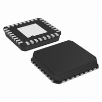
ADUC7061BCPZ32-RL Analog Devices Inc, ADUC7061BCPZ32-RL Datasheet - Page 38

ADUC7061BCPZ32-RL
Manufacturer Part Number
ADUC7061BCPZ32-RL
Description
DUAL 24-BIT AFE AND ARM 7 I.C
Manufacturer
Analog Devices Inc
Series
MicroConverter® ADuC7xxxr
Datasheet
1.EVAL-ADUC7061MKZ.pdf
(108 pages)
Specifications of ADUC7061BCPZ32-RL
Design Resources
USB Based Temperature Monitor Using ADuC7061 and an External RTD (CN0075) 4 mA-to-20 mA Loop-Powered Temperature Monitor Using ADuC7060/1 (CN0145)
Core Processor
ARM7
Core Size
16/32-Bit
Speed
10MHz
Connectivity
I²C, SPI, UART/USART
Peripherals
POR, PWM, Temp Sensor, WDT
Number Of I /o
8
Program Memory Size
32KB (32K x 8)
Program Memory Type
FLASH
Ram Size
4K x 8
Voltage - Supply (vcc/vdd)
2.375 V ~ 2.625 V
Data Converters
A/D 5x24b, 8x24b, D/A 1x14b
Oscillator Type
Internal
Operating Temperature
-40°C ~ 125°C
Package / Case
32-LFCSP
Lead Free Status / RoHS Status
Lead free / RoHS Compliant
Eeprom Size
-
Lead Free Status / RoHS Status
Lead free / RoHS Compliant
ADC
Register
Status
Chop On
Chop Off
Chop Off
Chop Off
ADuC7060/ADuC7061
Table 36. Primary ADC—Typical Output RMS Noise in Normal Mode (μV)
ADC
Register
Status
Chop On
Chop Off
Chop Off
Chop Off
Table 37. Primary ADC—Typical Output RMS Effective Number of Bits in Normal Mode (Peak-to-Peak Bits in Parentheses)
Table 38. Auxilary ADC—Typical Output RMS Noise
ADC Register
Chop On
Chop On
Chop Off
Chop Off
REFERENCE SOURCES
Both the primary and auxiliary ADCs have the option of using
the internal reference voltage or one of two external differential
reference sources. The first external reference is applied to the
VREF+/VREF− pins. The second external reference is applied
to the ADC4/EXT_REF2IN+ and ADC5/EXT_REF2IN− pins.
By default, each ADC uses the internal 1.2 V reference source.
For details on how to configure the external reference source for
the primary ADC, see the description of the ADC0REF[1:0]
bits in the ADC0 control register, ADC0CON.
For details on how to configure the external reference source for
the auxiliary ADC, see the description of the ADC1REF[2:0]
bits in the ADC1 control register, ADC1CON.
If an external reference source of greater than 1.35 V is needed
for ADC0, the HIGHEXTREF0 bit must be set in ADC0CON.
Data
Update
Rate
4 Hz
50 Hz
1 kHz
8 kHz
4 Hz
50 Hz
1 kHz
8 kHz
Data
Update
Rate
±1.2 V
(PGA = 1)
21.9
(19.1 p-p)
20.2
(17.5 p-p)
18.1
(15.3 p-p)
15.4
(12.7 p-p)
Data
Update Rate
4 Hz
10 Hz
1 kHz
8 kHz
±1.2 V
(PGA = 1)
0.62 μV
1.97 μV
8.54 μV
54.97 μV
±600 mV
(PGA = 2)
20.8
(18.1 p-p)
19.3
(16.6 p-p)
17.1
(14.4 p-p)
14.4
(11.7 p-p)
±600 mV
(PGA = 2)
0.648 μV
1.89 μV
8.4 μV
55.54 μV
RMS Value
0.633
0.810
7.4
54.18
±300 mV
(PGA = 4)
21.7
(19.0 p-p)
20.0
(17.3 p-p)
17.8
(15.1 p-p)
15.4
(12.6 p-p)
μ
±300 mV
(PGA = 4)
0.175 μV
0.570 μV
2.55 μV
14.30 μV
V
μ
μ
μ
V
V
V
±150 mV
(PGA = 8)
21.4
(18.7 p-p)
19.6
(16.9 p-p)
17.5
(14.8 p-p)
15.2
(12.5 p-p)
±150 mV
(PGA = 8)
0.109 μV
0.38 μV
1.6 μV
7.88 μV
Rev. B | Page 38 of 108
±75 mV
(PGA = 16)
20.9
(18.2 p-p)
19.1
(16.4 p-p)
17.0
(14.2 p-p)
15.0
(12.3 p-p)
Input Voltage Noise (mV)
±75 mV
(PGA = 16)
0.077 μV
0.27 μV
1.17 μV
4.59 μV
Input Voltage Noise (mV)
Similarly, if an external reference source of greater than 1.35 V
is used for ADC1, the HIGHEXTREF1 bit must be set in
ADC1CON.
DIAGNOSTIC CURRENT SOURCES
To detect a connection failure to an external sensor, the ADuC706x
incorporates a 50 μA constant current source on the selected
analog input channels to both the primary and auxiliary ADCs.
The diagnostic current sources for the primary ADC analog
inputs are controlled by the ADC0DIAG[1:0] bits in the
ADC0CON register.
Similarly, the diagnostic current sources for the auxiliary ADC
analog inputs are controlled by the ADC1DIAG[1:0] bits in the
ADC1CON register.
±37.5 mV
(PGA = 32)
20.8
(18.1 p-p)
19.0
(16.2 p-p)
16.8
(14.1 p-p)
14.9
(12.2 p-p)
±37.5 mV
(PGA = 32)
0.041 μV
0.147 μV
0.658 μV
2.5 μV
Figure 15. Example Circuit Using Diagnostic Current Sources
AVDD
±18.75 mV
(PGA = 64)
18.2
(15.5 p-p)
20.2
(17.4 p-p)
16.1
(13.4 p-p)
14.4
(11.7 p-p)
0.123 μV
±18.75 mV
(PGA = 64)
0.032 μV
0.53 μV
1.71 μV
A
A
R1
R2
B
B
±9.375 mV
(PGA = 128)
19.1
(16.4 p-p)
17.3
(14.6 p-p)
15.1
(12.3 p-p)
13.4
(10.7 p-p)
ADC0 (+)
ADC1 (–)
±9.375 mV
(PGA = 128)
0.0338 μV
0.12 μV
0.55 μV
1.75 μV
±4.68 mV
(PGA = 256)
18.2
(15.4 p-p)
16.6
(13.8 p-p)
14.0
(11.3 p-p)
13.3
(10.6 p-p)
±4.68 mV
(PGA = 256)
0.032 μV
0.098 μV
0.56 μV
0.915 μV
VIN =
ADC0,
ADC1
±2.34 mV
(PGA = 512)
17.1
(14.4 p-p)
15.5
(12.8 p-p)
13.1
(10.4 p-p)
12.3
(9.6 p-p)
±2.34 mV
(PGA = 512)
0.033 μV
0.098 μV
0.52 μV
0.909 μV


