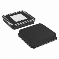
ADUC7061BCPZ32-RL Analog Devices Inc, ADUC7061BCPZ32-RL Datasheet - Page 74

ADUC7061BCPZ32-RL
Manufacturer Part Number
ADUC7061BCPZ32-RL
Description
DUAL 24-BIT AFE AND ARM 7 I.C
Manufacturer
Analog Devices Inc
Series
MicroConverter® ADuC7xxxr
Datasheet
1.EVAL-ADUC7061MKZ.pdf
(108 pages)
Specifications of ADUC7061BCPZ32-RL
Design Resources
USB Based Temperature Monitor Using ADuC7061 and an External RTD (CN0075) 4 mA-to-20 mA Loop-Powered Temperature Monitor Using ADuC7060/1 (CN0145)
Core Processor
ARM7
Core Size
16/32-Bit
Speed
10MHz
Connectivity
I²C, SPI, UART/USART
Peripherals
POR, PWM, Temp Sensor, WDT
Number Of I /o
8
Program Memory Size
32KB (32K x 8)
Program Memory Type
FLASH
Ram Size
4K x 8
Voltage - Supply (vcc/vdd)
2.375 V ~ 2.625 V
Data Converters
A/D 5x24b, 8x24b, D/A 1x14b
Oscillator Type
Internal
Operating Temperature
-40°C ~ 125°C
Package / Case
32-LFCSP
Lead Free Status / RoHS Status
Lead free / RoHS Compliant
Eeprom Size
-
Lead Free Status / RoHS Status
Lead free / RoHS Compliant
ADuC7060/ADuC7061
PULSE-WIDTH MODULATOR
PULSE-WIDTH MODULATOR GENERAL OVERVIEW
Each ADuC706x integrates a 6-channel pulse-width modulator
(PWM) interface. The PWM outputs can be configured to drive
an H-bridge or can be used as standard PWM outputs. On
power-up, the PWM outputs default to H-bridge mode. This
ensures that the motor is turned off by default. In standard
PWM mode, the outputs are arranged as three pairs of PWM
pins. Users have control over the period of each pair of outputs
and over the duty cycle of each individual output.
Table 83. PWM MMRs
MMR Name
PWMCON
PWM0COM0
PWM0COM1
PWM0COM2
PWM0LEN
PWM1COM0
PWM1COM1
PWM1COM2
PWM1LEN
PWM2COM0
PWM2COM1
PWM2COM2
PWM2LEN
PWMCLRI
Description
PWM control.
Compare Register 0 for PWM Output 0 and
PWM Output 1.
Compare Register 1 for PWM Output 0 and
PWM Output 1.
Compare Register 2 for PWM Output 0 and
PWM Output 1.
Frequency control for PWM Output 0 and PWM
Output 1.
Compare Register 0 for PWM Output 2 and
PWM Output 3.
Compare Register 1 for PWM Output 2 and
PWM Output 3.
Compare Register 2 for PWM Output 2 and
PWM Output 3.
Frequency control for PWM Output 2 and PWM
Output 3.
Compare Register 0 for PWM Output 4 and
PWM Output 5.
Compare Register 1 for PWM Output 4 and
PWM Output 5.
Compare Register 2 for PWM Output 4 and
PWM Output 5.
Frequency control for PWM Output 4 and PWM
Output 5.
PWM interrupt clear.
Rev. B | Page 74 of 108
In all modes, the PWMxCOMx MMRs control the point at
which the PWM outputs change state. An example of the first
pair of PWM outputs (PWM0 and PWM1) is shown in
The PWM clock is selectable via PWMCON with one of the
following values: UCLK divided by 2, 4, 8, 16, 32, 64, 128, or
256. The length of a PWM period is defined by PWMxLEN.
The PWM waveforms are set by the count value of the 16-bit
timer and the compare registers contents, as shown with the
PWM0 and PWM1 waveforms in
The low-side waveform, PWM1, goes high when the timer
count reaches PWM0LEN, and it goes low when the timer
count reaches the value held in PWM0COM2 or when the
high-side waveform (PWM0) goes low.
The high-side waveform, PWM0, goes high when the timer
count reaches the value held in PWM0COM0, and it goes low
when the timer count reaches the value held in PWM0COM1.
PWMCON Control Register
Name:
Address:
Default value:
Access:
Function:
HIGH SIDE
LOW SIDE
(PWM0)
(PWM1)
PWM0COM2
PWM0COM1
PWM0COM0
PWM0LEN
PWMCON
0xFFFF0F80
0x0012
Read and write
This is a 16-bit MMR that configures the
PWM outputs.
Figure 26. PWM Timing
Figure 26.
Figure 26.


