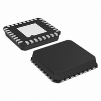
ADUC7061BCPZ32-RL Analog Devices Inc, ADUC7061BCPZ32-RL Datasheet - Page 36

ADUC7061BCPZ32-RL
Manufacturer Part Number
ADUC7061BCPZ32-RL
Description
DUAL 24-BIT AFE AND ARM 7 I.C
Manufacturer
Analog Devices Inc
Series
MicroConverter® ADuC7xxxr
Datasheet
1.EVAL-ADUC7061MKZ.pdf
(108 pages)
Specifications of ADUC7061BCPZ32-RL
Design Resources
USB Based Temperature Monitor Using ADuC7061 and an External RTD (CN0075) 4 mA-to-20 mA Loop-Powered Temperature Monitor Using ADuC7060/1 (CN0145)
Core Processor
ARM7
Core Size
16/32-Bit
Speed
10MHz
Connectivity
I²C, SPI, UART/USART
Peripherals
POR, PWM, Temp Sensor, WDT
Number Of I /o
8
Program Memory Size
32KB (32K x 8)
Program Memory Type
FLASH
Ram Size
4K x 8
Voltage - Supply (vcc/vdd)
2.375 V ~ 2.625 V
Data Converters
A/D 5x24b, 8x24b, D/A 1x14b
Oscillator Type
Internal
Operating Temperature
-40°C ~ 125°C
Package / Case
32-LFCSP
Lead Free Status / RoHS Status
Lead free / RoHS Compliant
Eeprom Size
-
Lead Free Status / RoHS Status
Lead free / RoHS Compliant
ADuC7060/ADuC7061
Table 33. ADuC706x Power Saving Modes
POWCON0[6:3]
1111
1110
1100
1000
0000
Table 34. Typical Current Consumption at 25°C in mA
POWCON0[6:3]
1111
1110
1100
1000
0000
1
2
3
Name:
Address:
Default value:
Access:
Function:
Name:
Address:
Default value:
Access:
Function:
All values listed in Table 34 have been taken with both ADCs turned off.
In active mode, GP0PAR bit 7 =1.
The values for pause, nap, sleep, and stop modes are measured with the NTRST pin low. To minimize I
the internal pull-down on the nTRST pin and means there is no ground path for the external pull-up resistor through the nTRST pin. By default, GP0PAR Bit 7 = 0,
therefore, setting this bit in user code will not affect the BM operation.
PLLKEY1
0xFFFF0410
0xXXXX
Write
When writing to the PLLCON register, the
value of 0xAA must be written to this register
in the instruction immediately before writing
to PLLCON.
PLLCON
0xFFFF0414
0x00
Read and write
This register selects the clock input to the PLL.
Active
Pause
Nap
Sleep
Stop
Mode
Mode
Active
Pause
Nap
Sleep
Stop
Core
Yes
3
3
3
3
2
Peripherals
Yes
Yes
CD = 0
5.22
2.6
1.33
0.085
0.055
CD = 1
4.04
1.95
1.29
0.085
0.055
PLL
Yes
Yes
Yes
1
Rev. B | Page 36 of 108
XTAL/T2/T3
Yes
Yes
Yes
Yes
CD = 2
2.69
1.6
1.29
0.085
0.055
Table 35. PLLCON MMR Bit Designations
Bit
7:3
2
1:0
Name:
Address:
Default value:
Access:
Function:
Name
Reserved
EXTCLK
OSEL
CD = 3
2.01
1.49
1.29
0.085
0.055
IRQ0 to IRQ3
Yes
Yes
Yes
Yes
Yes
DD
due to nTRST in all modes, set GP0PAR Bit 7 =1. This disables
PLLKEY2
0xFFFF0418
0xXXXX
Write
When writing to PLLCON, the value of 0x55
must be written to this register in the
instruction immediately after writing to
PLLCON.
CD = 4
1.67
1.4
1.29
0.085
0.055
Description
These bits must always be set to 0.
Set this bit to 1 to select external clock input
from P2.0.
Clear this bit to disable the external clock.
Oscillator selection bits.
[00] = internal 32,768 Hz oscillator.
[01] = internal 32,768 Hz oscillator.
[10] = external crystal.
[11] = internal 32,768 Hz oscillator.
Start-Up/Power-On Time
130 ms at CD = 0
4.8 μs at CD = 0; 660 μs at CD = 7
4.8 μs at CD = 0; 660 μs at CD = 7
66 μs at CD = 0; 900 μs at CD = 7
66 μs at CD = 0; 900 μs at CD = 7
CD = 5
1.51
1.33
1.29
0.085
0.055
CD = 6
1.42
1.31
1.29
0.085
0.055
CD = 7
1.38
1.3
1.29
0.085
0.055


