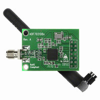
EVAL-ADF7021-NDBZ2 Analog Devices Inc, EVAL-ADF7021-NDBZ2 Datasheet - Page 23

EVAL-ADF7021-NDBZ2
Manufacturer Part Number
EVAL-ADF7021-NDBZ2
Description
860 MHz To 870 MHz
Manufacturer
Analog Devices Inc
Type
Transceiver, FSKr
Datasheet
1.ADF7021-NBCPZ-RL.pdf
(64 pages)
Specifications of EVAL-ADF7021-NDBZ2
Frequency
860MHz ~ 870MHz
Lead Free Status / RoHS Status
Lead free / RoHS Compliant
For Use With/related Products
ADF7021-N
Lead Free Status / RoHS Status
Lead free / RoHS Compliant
EVAL-ADF7021-NDBxx should be used for optimum
performance.
The free design tool ADI SRD Design Studio™ can also
be used to design loop filters for the ADF7021-N (see the ADI
SRD Design Studio
N Counter
The feedback divider in the ADF7021-N PLL consists of an
8-bit integer counter (R0_DB[19:26]) and a 15-bit, sigma-delta
(Σ-Δ) fractional_N divider (R0_DB[4:18]). The integer counter
is the standard pulse-swallow type that is common in PLLs. This
sets the minimum integer divide value to 23. The fractional divide
value provides very fine resolution at the output, where the output
frequency of the PLL is calculated as
When RF_DIVIDE_BY_2 (see the Voltage Controlled
Oscillator (VCO) section) is selected, this formula becomes
The combination of Integer_N (maximum = 255) and
Fractional_N (maximum = 32,768/32,768) gives a maximum
N divider of 255 + 1. Therefore, the minimum usable PFD is
For example, when operating in the European 868 MHz to
870 MHz band, PFD
Voltage Regulators
The ADF7021-N contains four regulators to supply stable
voltages to the part. The nominal regulator voltage is 2.3 V.
Regulator 1 requires a 3.9 Ω resistor and a 100 nF capacitor in
series between CREG1 and GND, whereas the other regulators
require a 100 nF capacitor connected between CREGx and GND.
When CE is high, the regulators and other associated circuitry
are powered on, drawing a total supply current of 2 mA. Bringing
the CE pin low disables the regulators, reduces the supply current
to less than 1 μA, and erases all values held in the registers.
The serial interface operates from a regulator supply. Therefore,
to write to the part, the user must have CE high and the regulator
PFD
REFERENCE IN
f
f
OUT
OUT
4\R
MIN
=
=
XTAL
XTAL
[ ]
Hz
R
R
CHARGE
FRACTIONAL_N
PUMP
PFD/
=
web site for details).
×
×
Figure 35. Fractional_N PLL
MIN
Maximum
⎛
⎜ ⎜
⎝
0.5
Integer
= 3.4 MHz.
×
⎛
⎜
⎝
Integer_N
Σ-Δ MODULATOR
THIRD-ORDER
_
Required
N
+
(
Fractional
255
+
Fractional
+
Output
2
INTEGER_N
1
15
)
VCO
4\N
2
_
15
N
Frequency
_
⎞
⎟ ⎟
⎠
N
⎞
⎟
⎠
Rev. 0 | Page 23 of 64
voltage must be stabilized. Regulator status (CREG4) can be
monitored using the REGULATOR_READY signal from the
MUXOUT pin.
MUXOUT
The MUXOUT pin allows access to various digital points in the
ADF7021-N. The state of MUXOUT is controlled in Register 0
(R0_DB[29:31]).
REGULATOR_READY
REGULATOR_READY is the default setting on MUXOUT
after the transceiver is powered up. The power-up time of the
regulator is typically 50 μs. Because the serial interface is powered
from the regulator, the regulator must be at its nominal voltage
before the ADF7021-N can be programmed. The status of the
regulator can be monitored at MUXOUT. When the regulator
ready signal on MUXOUT is high, programming of the
ADF7021-N can begin.
FILTER_CAL_COMPLETE
MUXOUT can be set to FILTER_CAL_COMPLETE. This signal
goes low for the duration of both a coarse IF filter calibration
and a fine IF filter calibration. It can be used as an interrupt to
a microcontroller to signal the end of the IF filter calibration.
DIGITAL_LOCK_DETECT
DIGITAL_LOCK_DETECT indicates when the PLL has locked.
The lock detect circuit is located at the PFD. When the phase
error on five consecutive cycles is less than 15 ns, lock detect is
set high. Lock detect remains high until a 25 ns phase error is
detected at the PFD.
RSSI_READY
MUXOUT can be set to RSSI_READY. This indicates that the
internal analog RSSI has settled and a digital RSSI readback can
be performed.
Tx_Rx
Tx_Rx signifies whether the ADF7021-N is in transmit or receive
mode. When in transmit mode, this signal is low. When in receive
mode, this signal is high. It can be used to control an external
Tx/Rx switch.
REGULATOR_READY (DEFAULT)
FILTER_CAL_COMPLETE
DIGITAL_LOCK_DETECT
LOGIC_ZERO
RSSI_READY
LOGIC_ONE
TRISTATE
Tx_Rx
Figure 36. MUXOUT Circuit
MUX
CONTROL
ADF7021-N
DGND
DV
DD
MUXOUT


