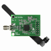
EVAL-ADF7021-NDBZ2 Analog Devices Inc, EVAL-ADF7021-NDBZ2 Datasheet - Page 31

EVAL-ADF7021-NDBZ2
Manufacturer Part Number
EVAL-ADF7021-NDBZ2
Description
860 MHz To 870 MHz
Manufacturer
Analog Devices Inc
Type
Transceiver, FSKr
Datasheet
1.ADF7021-NBCPZ-RL.pdf
(64 pages)
Specifications of EVAL-ADF7021-NDBZ2
Frequency
860MHz ~ 870MHz
Lead Free Status / RoHS Status
Lead free / RoHS Compliant
For Use With/related Products
ADF7021-N
Lead Free Status / RoHS Status
Lead free / RoHS Compliant
The user has the option of changing the two threshold values
from the defaults of 30 and 70 (Register 9). The default AGC
setup values should be adequate for most applications. The
threshold values must be more than 30 apart for the AGC to
operate correctly.
Offset Correction Clock
In Register 3, the user should set the BBOS_CLK_DIVIDE bits
(R3_DB[4:5]) to give a baseband offset clock (BBOS CLK)
frequency between 1 MHz and 2 MHz.
where BBOS_CLK_DIVIDE can be set to 4, 8, 16, or 32.
AGC Information and Timing
AGC is selected by default and operates by setting the appropriate
LNA and filter gain settings for the measured RSSI level. It is
possible to disable AGC by writing to Register 9 if the user wants to
enter one of the modes listed in Table 15. The time for the AGC
circuit to settle and, therefore, the time it takes to measure the RSSI
accurately, is typically 390 μs. However, this depends on how many
gain settings the AGC circuit has to cycle through. After each gain
change, the AGC loop waits for a programmed time to allow
transients to settle. This AGC update rate is set according to
where:
AGC_CLK_DIVIDE is set by R3_DB[26:31]. A value of 13 is
recommended.
SEQ_CLK_DIVIDE = 100 kHz (R3_DB[18:25]).
Table 15. LNA/Mixer Modes
Receiver Mode
High Sensitivity
Mode (Default)
Enhanced Linearity
High Gain
Medium Gain
Enhanced Linearity
Medium Gain
Low Gain
Enhanced Linearity
Low Gain
BBOS CLK [Hz] = XTAL/(BBOS_CLK_DIVIDE)
AGC Update Rate [Hz] =
LNA_MODE
(R9_DB25)
0
0
1
1
1
1
SEQ
AGC
_
LNA_GAIN
(R9_DB[20:21])
30
30
10
10
3
3
CLK
_
CLK
_
DIVIDE
_
DIVIDE
[Hz]
MIXER_LINEARITY
(R9_DB28)
0
1
0
1
0
1
Rev. 0 | Page 31 of 64
By using the recommended setting for AGC_CLK_DIVIDE, the
total AGC settling time is
The worst case for AGC settling occurs when the AGC control
loop has to cycle through all five gain settings, which gives a
maximum AGC settling time of 650 μs.
RSSI Formula (Converting to dBm)
The RSSI formula is
where:
Readback Code is given by Bit RV7 to Bit RV1 in the Register 7
readback register (see Figure 58 and the Readback Format
section).
Gain Mode Correction is given by the values in Table 14.
The LNA gain (LG2, LG1) and filter gain (FG2, FG1) values
are also obtained from the readback register, as part of an RSSI
readback.
Table 14. Gain Mode Correction
LNA Gain
(LG2, LG1)
H (1, 0)
M (0, 1)
M (0, 1)
M (0, 1)
L (0, 0)
An additional factor should be introduced to account for losses
in the front-end-matching network/antenna.
Sensitivity (2FSK, DR =
4.8 kbps, f
−118
−114.5
−112
−105.5
−100
−92.3
Input Power [dBm] = −130 dBm + (Readback Code + Gain
AGC
Mode Correction) × 0.5
Settling
DEV
= 4 kHz)
Time
Filter Gain
(FG2, FG1)
H (1, 0)
H (1, 0)
M (0, 1)
L (0, 0)
L (0, 0)
[sec]
=
Rx Current
Consumption (mA)
24.6
24.6
22.1
22.1
22.1
22.1
Number
AGC
of
Update
AGC
Gain Mode
Correction
0
24
38
58
86
ADF7021-N
Gain
Rate
[Hz]
Changes
Input IP3
(dBm)
−24
−20
−13.5
−9
−5
−3


