AD9912/PCBZ Analog Devices Inc, AD9912/PCBZ Datasheet - Page 3
AD9912/PCBZ
Manufacturer Part Number
AD9912/PCBZ
Description
Eval Board
Manufacturer
Analog Devices Inc
Series
AgileRF™r
Specifications of AD9912/PCBZ
Kit Features
Flexible System Clock I/P Accepts Crystal
Supported Devices
AD9912
Tool / Board Applications
Direct Digital Synthesizer
Development Tool Type
Hardware - Eval/Demo Board
Mcu Supported Families
AD9912
Main Purpose
Timing, Direct Digital Synthesis (DDS)
Embedded
No
Utilized Ic / Part
AD9912
Primary Attributes
14-Bit DAC, 48-Bit Tuning Word Width
Secondary Attributes
1GHz, Graphical User Interface
Lead Free Status / RoHS Status
Lead free / RoHS Compliant
Lead Free Status / RoHS Status
Lead free / RoHS Compliant, Lead free / RoHS Compliant


EVALUATION BOARD PHYSICAL CONNECTIONS
The following instructions are for setting up the physical
connections to the
the evaluation software has already been installed. The physical
connections for Revision A and Revision B of the AD9912
evaluation board are identical.
The following case is used as an example: output frequency:
155.52 MHz; DAC system clock: 1000 MHz input provided on
the SYSCLK SMA connector; system clock PLL is disabled.
POWER CONNECTIONS
1.
2.
3.
4.
5.
6.
Connect power and ground to the main power connector
labeled TB1, and follow the silkscreen labels describing
each power connection.
Connect a 1.8 V supply to VDD_DACDEC (J32).
Connect a 3.3 V supply to the following AD9912 SMA
connectors: VDD_DAC3 (J11) and XO_PWR (J12)
(XO_PWR is only necessary if there is a crystal oscillator
mounted on the board).
If using the CMOS OUT (J7), power must also be applied
to VDDX_DRV (J9), and R106 must be populated with a
0 Ω resistor. VDDX_DRV can be either 1.8 V or 3.3 V.
Note that the power-on default of the AD9912 is CMOS
driver enabled, HSTL driver disabled.
Ensure that the S1 to S4 jumpers are tied to VDD. These
settings are only for generating 155.52 MHz at startup and
register programming overrides these settings.
Apply power.
AD9912
evaluation board. They assume that
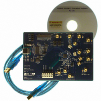
Figure 2. AD9912 Evaluation Board, Rev. A
Rev. 0 | Page 3 of 12
Note that there are two other 1.8 V power connectors,
VDD_DACCLK (J16) and VDD_DRV/VDD_FDBK (J17),
on the evaluation board. These power supplies are fed by the
AVDD supply on connector TB1 when the following 0 Ω
resistors are in place (on the back of the board): R9, R10, R23,
R60, R63, R64, R65, R66, R19, R22, and R132.
CONNECTIONS TO PC
1.
2.
SIGNAL CONNECTIONS
1.
2.
3.
Connect the USB cables to the evaluation board and the
computer. The LED labeled USB on the AD9912 evaluation
board should be blinking.
See the Evaluation Board Software Setup section for details
on running the AD9912 evaluation board software.
Ensure that JMP1 connects VDD to the center pin.
Connect the 1 GHz signal generator to SYSCLK (J10). An
amplitude setting of 0 dBm to +3 dBm is fine. If a crystal
oscillator is used for generating SYSCLK, the SYSCLK
(J10) input can be left open.
The user has the following four output options on the
AD9912:
•
CMOS driver (default): connect an oscilloscope/
spectrum analyzer to CMOS_OUT (J7). Note that
R106 must be installed to connect J7 to the CMOS out
on the AD9912. Connect DUT FILTER OUT (J5) to
FDBK IN (J6). Note that this step is not necessary if
R20 (near J5) and R18 (near FDBK IN/J6) are stuffed.
AD9912/PCBZ
Related parts for AD9912/PCBZ
Image
Part Number
Description
Manufacturer
Datasheet
Request
R


Part Number:
Description:
±1.7g Dual-Axis IMEMS Accelerometer Evaluation Board
Manufacturer:
Analog Devices Inc
Datasheet:

Part Number:
Description:
Inertial Sensor Evaluation System
Manufacturer:
Analog Devices Inc
Datasheet:
Part Number:
Description:
Manufacturer:
Analog Devices Inc
Datasheet:
Part Number:
Description:
Manufacturer:
Analog Devices Inc
Datasheet:
Part Number:
Description:
Manufacturer:
Analog Devices Inc
Datasheet:
Part Number:
Description:
Manufacturer:
Analog Devices Inc
Datasheet:
Part Number:
Description:
Manufacturer:
Analog Devices Inc
Datasheet:
Part Number:
Description:
Manufacturer:
Analog Devices Inc
Datasheet:
Part Number:
Description:
Manufacturer:
Analog Devices Inc
Datasheet:
Part Number:
Description:
Manufacturer:
Analog Devices Inc
Datasheet:
Part Number:
Description:
Manufacturer:
Analog Devices Inc
Datasheet:
Part Number:
Description:
Manufacturer:
Analog Devices Inc
Datasheet: