AD9912/PCBZ Analog Devices Inc, AD9912/PCBZ Datasheet - Page 8
AD9912/PCBZ
Manufacturer Part Number
AD9912/PCBZ
Description
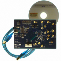
Eval Board
Manufacturer
Analog Devices Inc
Series
AgileRF™r
Specifications of AD9912/PCBZ
Kit Features
Flexible System Clock I/P Accepts Crystal
Supported Devices
AD9912
Tool / Board Applications
Direct Digital Synthesizer
Development Tool Type
Hardware - Eval/Demo Board
Mcu Supported Families
AD9912
Main Purpose
Timing, Direct Digital Synthesis (DDS)
Embedded
No
Utilized Ic / Part
AD9912
Primary Attributes
14-Bit DAC, 48-Bit Tuning Word Width
Secondary Attributes
1GHz, Graphical User Interface
Lead Free Status / RoHS Status
Lead free / RoHS Compliant
Lead Free Status / RoHS Status
Lead free / RoHS Compliant, Lead free / RoHS Compliant


AD9912/PCBZ
EVALUATION SOFTWARE FUNCTIONAL BLOCKS
The
correspond to the AD9912’s major functional blocks. These
subsections are listed in the following sections, and each of these
has its own window.
The main window is the Interactive Block Diagram window,
and from it, the window for each functional block can be
accessed by clicking that block. The user can also access each of
these windows from the Window menu at the top of the
window.
Each window has a check box labeled Auto I/O Update. If this
box is checked, the software performs an I/O update operation
any time there is a setting change in that box.
For convenience, some detailed information from the AD9912
data sheet is included here. In cases where there is an inconsis-
tency between this document and the AD9912 data sheet,
assume that the data sheet is correct. Please inform us of this
inconsistency so that it can be corrected.
INTERACTIVE BLOCK DIAGRAM
The Interactive Block Diagram (IBD) window shows all of the
major blocks of the chip, and clicking a block, such as DDS,
brings up a window where the user can change the settings for
that block.
S-DIVIDER SETTINGS WINDOW
Clicking the S-Divider box brings up the S-Divider Settings
window.
This window is used for setting the output divider for the CMOS
output and for setting the divide-by-2 prescaler. Note that this
bit must be set if the signal present on FDBK_IN is 400 MHz or
greater.
DDS AND CLOCK MULTIPLIER CONTROL
Clicking the DDS and Clock Multiplier box brings up the DDS
and Clock Multiplier window. This window is used to set up
the system clock PLL and is frequently used. It contains two
tabs: DDS and Harmonic Spur Reduction.
The DDS tab has three sections: DDS Clock, DDS Settings,
and DAC Control.
In the DDS Clock section of the tab, the frequency of the
external clock source driving the system clock is entered into
the box labeled External Clock. The default is 25 MHz. If the
system clock is supplied directly, be sure to put a check in the
Bypass Multiplier check box.
If the system clock PLL (SYSCLK PLL) is to be used, enter the
desired multiplication factor. The multiplier value in the panel
does not factor in the bipolar edge detector. Therefore, if an
overall multiplication factor of 40 is desired when using the
bipolar edge detector, ×20 should be entered for the multiplier.
It is recommended to put a check in the Auto Range check box.
This is especially true for system clocks in the 800 MHz to
AD9912
evaluation software is made up of subsections that
Rev. 0 | Page 8 of 12
900 MHz range. Refer to the AD9912 data sheet on the use of
VCO Auto Range.
The charge pump current of 250 μA (default) is fine for most
applications, but it can be adjusted here if desired.
The Clock Multiplier section has an ×2 Reference check box,
and it controls the bipolar edge detector of the system clock
PLL. This frequency doubler can reduce the in-band jitter of the
system clock PLL, and it is described in detail in the AD9912
data sheet. When this box is checked, the multiplier must be cut
in half to maintain the same overall frequency multiplication.
The desired output frequency is entered in the DDS Settings
section. Note that loading the DPLL settings that are generated
using FilterDesign.xls automatically sets the output frequency
calculated in FilterDesign.xls. The primary value of entering an
output frequency here is to set up single-tone mode without
having to configure the DPLL loop filter. The DDS Settings
section also features a place to enter a static phase offset. Bear in
mind that this static phase offset is not active when the DPLL
loop is closed.
DAC Control is the last section of the DDS tab. The DDS DAC
current can be altered here. However, the default values are
recommended, and these values are not normally altered.
Increasing the DAC current increases the output amplitude but
can degrade the harmonic performance of the DAC. One case
where this might be useful is when using a SAW filter because
they can have high insertion loss.
CMOS DRIVER AND CLOCK OUT
Clicking the mux symbol near the CMOS output driver in the
Interactive Block Diagram window brings up the CMOS
Driver and Clock Out window. Features that are accessed here
include the CMOS output divider, HSTL driver power-down,
and the HSTL output doubler.
STATUS AND IRQ CONTROL WINDOW
This feature is not applicable to the AD9912.
DEBUG WINDOW
Clicking the Debug button at the top of the evaluation software
window brings up the Debug window. This is a legacy window,
and the user should not normally need to access it.
The Serial I/O section of this window provides a handy way to
read and write registers directly.
Quick Edit provides an easy way to get a quick look at the
DPLL Registers and Settings. This includes the digital loop
filter coefficients, the dividers, and the frequency tuning word.
REGISTER MAP (REGMAP VALUES) WINDOW
Clicking RegMap Values in the Window menu brings up the
Register Map window. This is a handy text window for quickly
viewing the register map.
Related parts for AD9912/PCBZ
Image
Part Number
Description
Manufacturer
Datasheet
Request
R


Part Number:
Description:
±1.7g Dual-Axis IMEMS Accelerometer Evaluation Board
Manufacturer:
Analog Devices Inc
Datasheet:

Part Number:
Description:
Inertial Sensor Evaluation System
Manufacturer:
Analog Devices Inc
Datasheet:
Part Number:
Description:
Manufacturer:
Analog Devices Inc
Datasheet:
Part Number:
Description:
Manufacturer:
Analog Devices Inc
Datasheet:
Part Number:
Description:
Manufacturer:
Analog Devices Inc
Datasheet:
Part Number:
Description:
Manufacturer:
Analog Devices Inc
Datasheet:
Part Number:
Description:
Manufacturer:
Analog Devices Inc
Datasheet:
Part Number:
Description:
Manufacturer:
Analog Devices Inc
Datasheet:
Part Number:
Description:
Manufacturer:
Analog Devices Inc
Datasheet:
Part Number:
Description:
Manufacturer:
Analog Devices Inc
Datasheet:
Part Number:
Description:
Manufacturer:
Analog Devices Inc
Datasheet:
Part Number:
Description:
Manufacturer:
Analog Devices Inc
Datasheet: