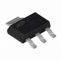
BSP030,115 NXP Semiconductors, BSP030,115 Datasheet - Page 5

BSP030,115
Manufacturer Part Number
BSP030,115
Description
MOSFET N-CH 30V 10A SOT223
Manufacturer
NXP Semiconductors
Series
TrenchMOS™r
Datasheet
1.BSP030115.pdf
(13 pages)
Specifications of BSP030,115
Package / Case
SOT-223 (3 leads + Tab), SC-73, TO-261
Mounting Type
Surface Mount
Power - Max
8.3W
Fet Type
MOSFET N-Channel, Metal Oxide
Gate Charge (qg) @ Vgs
40nC @ 10V
Vgs(th) (max) @ Id
2.8V @ 1mA
Current - Continuous Drain (id) @ 25° C
10A
Drain To Source Voltage (vdss)
30V
Fet Feature
Logic Level Gate
Rds On (max) @ Id, Vgs
30 mOhm @ 5A, 10V
Minimum Operating Temperature
- 65 C
Configuration
Single Dual Drain
Transistor Polarity
N-Channel
Resistance Drain-source Rds (on)
30 mOhms
Forward Transconductance Gfs (max / Min)
12 S
Drain-source Breakdown Voltage
43 V
Gate-source Breakdown Voltage
+/- 20 V
Continuous Drain Current
10 A
Power Dissipation
8.3 W
Maximum Operating Temperature
+ 150 C
Mounting Style
SMD/SMT
Lead Free Status / RoHS Status
Lead free / RoHS Compliant
Lead Free Status / RoHS Status
Lead free / RoHS Compliant, Lead free / RoHS Compliant
Other names
934043650115::BSP030 T/R::BSP030 T/R
8. Characteristics
Table 5:
T
Philips Semiconductors
9397 750 07268
Product specification
Symbol
Static characteristics
V
V
I
I
R
Dynamic characteristics
g
Q
Q
Q
C
C
C
t
t
t
t
t
t
DSS
GSS
d(on)
r
on
d(off)
f
off
j
fs
(BR)DSS
GS(th)
DSon
g(tot)
gs
gd
iss
oss
rss
= 25 C unless otherwise specified
Characteristics
Parameter
drain-source breakdown
voltage
gate-source threshold voltage I
drain-source leakage current
gate-source leakage current
drain-source on-state
resistance
forward transconductance
total gate charge
gate-source charge
gate-drain (Miller) charge
input capacitance
output capacitance
reverse transfer capacitance
turn-on delay time
turn-on rise time
turn-on time
turn-off delay time
turn-off fall time
turn-off time
Conditions
I
Figure 9
V
V
V
Figure 7
V
Figure 7
V
Figure 11
I
V
V
f = 1 MHz;
V
V
D
D
D
DS
GS
GS
GS
DS
GS
GS
DD
GS
T
T
T
T
T
T
T
T
T
T
= 10 A; V
= 1 mA; V
= 5 A; V
j
j
j
j
j
j
j
j
j
j
= 24 V; V
= 5 V; I
= 25 C
= 55 C
= 25 C
= 150 C
= 55 C
= 25 C
= 150 C
= 20 V; V
= 10 V; I
= 25 C
= 5 V; I
= 25 C
= 150 C
= 10 V;
= 0 V; V
= 15 V; R
= 10 V; R
Rev. 04 — 26 July 2000
and
and
DS
Figure 12
D
D
Figure 14
DS
DS
D
GS
8
8
= 5.5 A;
= 2.5 A;
= 15 V;
GS
D
G
= 5 A;
DS
= V
= 24 V;
= 15 ;
= 6
= 0 V
= 0 V
= 0 V
N-channel enhancement mode field-effect transistor
GS
;
Min
30
27
1
0.6
Typ
43
2
10
10
20
30
12
24
3.3
7.4
770
265
180
8
10
18
24
20
44
© Philips Electronics N.V. 2000. All rights reserved.
Max
2.8
3.5
100
10
100
30
50
85
40
35
150
BSP030
Unit
V
V
V
V
V
nA
nA
m
m
m
S
nC
nC
nC
pF
pF
pF
ns
ns
ns
ns
ns
ns
5 of 13
A


