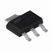
BSP030,115 NXP Semiconductors, BSP030,115 Datasheet - Page 8

BSP030,115
Manufacturer Part Number
BSP030,115
Description
MOSFET N-CH 30V 10A SOT223
Manufacturer
NXP Semiconductors
Series
TrenchMOS™r
Datasheet
1.BSP030115.pdf
(13 pages)
Specifications of BSP030,115
Package / Case
SOT-223 (3 leads + Tab), SC-73, TO-261
Mounting Type
Surface Mount
Power - Max
8.3W
Fet Type
MOSFET N-Channel, Metal Oxide
Gate Charge (qg) @ Vgs
40nC @ 10V
Vgs(th) (max) @ Id
2.8V @ 1mA
Current - Continuous Drain (id) @ 25° C
10A
Drain To Source Voltage (vdss)
30V
Fet Feature
Logic Level Gate
Rds On (max) @ Id, Vgs
30 mOhm @ 5A, 10V
Minimum Operating Temperature
- 65 C
Configuration
Single Dual Drain
Transistor Polarity
N-Channel
Resistance Drain-source Rds (on)
30 mOhms
Forward Transconductance Gfs (max / Min)
12 S
Drain-source Breakdown Voltage
43 V
Gate-source Breakdown Voltage
+/- 20 V
Continuous Drain Current
10 A
Power Dissipation
8.3 W
Maximum Operating Temperature
+ 150 C
Mounting Style
SMD/SMT
Lead Free Status / RoHS Status
Lead free / RoHS Compliant
Lead Free Status / RoHS Status
Lead free / RoHS Compliant, Lead free / RoHS Compliant
Other names
934043650115::BSP030 T/R::BSP030 T/R
Philips Semiconductors
9397 750 07268
Product specification
Fig 13. Source (diode forward) current as a function of
T
j
= 25 C and 150 C; V
source-drain (diode forward) voltage; typical
values.
(A)
I S
20
18
16
14
12
10
8
6
4
2
0
0
V GS = 0 V
0.2
0.4
GS
= 0 V
0.6
150 o C
0.8
Tj = 25 o C
V SD (V)
1
03ac29
1.2
Rev. 04 — 26 July 2000
N-channel enhancement mode field-effect transistor
Fig 14. Gate-source voltage as a function of gate
I
D
= 5 A; V
charge; typical values.
V GS
(V)
15
14
13
12
11
10
9
8
7
6
5
4
3
2
1
0
DS
0
= 15 V
I D = 5 A
V DS = 15 V
T j = 25 o C
5
10
15
© Philips Electronics N.V. 2000. All rights reserved.
20
25
Q G (nC)
BSP030
30
03ac31
35
8 of 13


