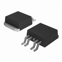
BUK7107-55AIE,118 NXP Semiconductors, BUK7107-55AIE,118 Datasheet - Page 5

BUK7107-55AIE,118
Manufacturer Part Number
BUK7107-55AIE,118
Description
MOSFET N-CH 55V 75A D2PAK
Manufacturer
NXP Semiconductors
Datasheet
1.BUK7907-55AIE127.pdf
(15 pages)
Specifications of BUK7107-55AIE,118
Fet Type
MOSFET N-Channel, Metal Oxide
Fet Feature
Current Sensing
Rds On (max) @ Id, Vgs
7 mOhm @ 50A, 10V
Drain To Source Voltage (vdss)
55V
Current - Continuous Drain (id) @ 25° C
75A
Vgs(th) (max) @ Id
4V @ 1mA
Gate Charge (qg) @ Vgs
116nC @ 10V
Input Capacitance (ciss) @ Vds
4500pF @ 25V
Power - Max
272W
Mounting Type
Surface Mount
Package / Case
D²Pak, TO-263 (4 leads + tab)
Configuration
Single
Transistor Polarity
N-Channel
Resistance Drain-source Rds (on)
0.007 Ohms
Drain-source Breakdown Voltage
55 V
Gate-source Breakdown Voltage
+/- 20 V
Continuous Drain Current
75 A
Power Dissipation
272 W
Maximum Operating Temperature
+ 175 C
Mounting Style
SMD/SMT
Minimum Operating Temperature
- 55 C
Lead Free Status / RoHS Status
Lead free / RoHS Compliant
Other names
934057272118
BUK7107-55AIE /T3
BUK7107-55AIE /T3
BUK7107-55AIE /T3
BUK7107-55AIE /T3
Philips Semiconductors
5. Characteristics
Table 4:
T
9397 750 09877
Product data
Symbol
Static characteristics
V
V
I
V
I
R
I
Dynamic characteristics
Q
Q
Q
C
C
C
t
t
t
t
L
L
DSS
GSS
D
d(on)
r
d(off)
f
j
d
s
(BR)DSS
GS(th)
(BR)GSS
DSon
iss
oss
rss
g(tot)
gs
gd
= 25 C unless otherwise specified.
/I
sense
Characteristics
Parameter
drain-source breakdown
voltage
gate-source threshold voltage I
drain-source leakage current
gate-source breakdown
voltage
gate-source leakage current
drain-source on-state
resistance
ratio of drain current to sense
current
total gate charge
gate-source charge
gate-to-drain (Miller) charge
input capacitance
output capacitance
reverse transfer capacitance
turn-on delay time
rise time
turn-off delay time
fall time
internal drain inductance
internal source inductance
Conditions
I
Figure 9
V
I
V
V
Figure 7
V
V
I
V
f = 1 MHz;
V
V
from upper edge of drain
mounting base to center of
die
from source lead to source
bond pad
D
D
G
D
55 C < T
55 C < T
GS
GS
DS
GS
GS
GS
DS
GS
T
T
T
T
T
T
T
T
T
T
T
= 0.25 mA; V
= 1 mA; V
= 25 A;
= 1 mA;
j
j
j
j
j
j
j
j
j
j
j
= 55 V; V
> 10 V;
= 10 V; V
= 30 V; R
= 25 C
= 55 C
= 25 C
= 175 C
= 55 C
= 25 C
= 175 C
= 10 V; V
= 25 C
= 175 C
= 10 V; I
= 25 C
= 175 C
= 0 V; V
= 10 V; R
Rev. 01 — 12 August 2002
and
j
j
Figure 14
Figure 12
<175 C
<175 C
DS
DS
D
8
GS
DS
L
G
= 50 A;
DS
= V
= 1.2 ;
GS
= 25 V;
= 10
= 0 V
= 44 V;
= 0 V
= 0 V
GS
;
Min
55
50
2
1
-
-
-
20
-
-
-
-
450
-
-
-
-
-
-
-
-
-
-
-
-
BUK71/7907-55AIE
TrenchPLUS standard level FET
© Koninklijke Philips Electronics N.V. 2002. All rights reserved.
Typ
-
-
3
-
-
0.1
-
22
22
-
5.8
-
500
116
19
50
4500
960
510
36
115
159
111
2.5
7.5
Max
-
-
4
-
4.4
10
250
-
1000
10
7
14
550
-
-
-
-
-
-
-
-
-
-
-
-
Unit
V
V
V
V
V
V
nA
m
m
nC
nC
nC
pF
pF
pF
ns
ns
ns
ns
nH
nH
5 of 15
A
A
A


