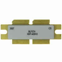
BLF574,112 NXP Semiconductors, BLF574,112 Datasheet - Page 14

BLF574,112
Manufacturer Part Number
BLF574,112
Description
TRANSISTOR RF LDMOS SOT539A
Manufacturer
NXP Semiconductors
Datasheet
1.BLF574112.pdf
(18 pages)
Specifications of BLF574,112
Package / Case
SOT539A
Transistor Type
LDMOS
Frequency
225MHz
Gain
26.5dB
Voltage - Rated
110V
Current Rating
56A
Current - Test
1A
Voltage - Test
50V
Power - Output
400W
Forward Transconductance Gfs (max / Min)
17 S
Mounting Style
SMD/SMT
Resistance Drain-source Rds (on)
0.14 Ohms
Drain-source Breakdown Voltage
110 V
Gate-source Breakdown Voltage
11 V
Continuous Drain Current
56 A
Power Dissipation
500 W
Application
HF/VHF
Channel Type
N
Channel Mode
Enhancement
Drain Source Voltage (max)
110V
Output Power (max)
600W
Power Gain (typ)@vds
26.5@50VdB
Frequency (max)
500MHz
Package Type
LDMOST
Pin Count
5
Forward Transconductance (typ)
17S
Drain Source Resistance (max)
90(Typ)@6Vmohm
Input Capacitance (typ)@vds
300@50VpF
Output Capacitance (typ)@vds
72@50VpF
Reverse Capacitance (typ)
1.5@50VpF
Operating Temp Range
-65C to 225C
Drain Efficiency (typ)
70%
Mounting
Screw
Mode Of Operation
CW
Number Of Elements
2
Vswr (max)
13
Screening Level
Military
Lead Free Status / RoHS Status
Lead free / RoHS Compliant
Noise Figure
-
Lead Free Status / Rohs Status
Lead free / RoHS Compliant
Other names
568-4736
934061965112
934061965112
NXP Semiconductors
BLF574_2
Product data sheet
Fig 15. Class-AB common-source production test circuit
Fig 16. Component layout for class-AB production test circuit
input
50
T1
T2
T1
T2
11 mm
C1
C2
C1
C2
C3
C3
C4 C5
C4 C5
37 mm
L6
L5
Rev. 02 — 24 February 2009
C8
C7
C6
C9
C8
C7
C6
C9
V
V
L8
L7
GG
GG
R2
R1
R2
R1
R3
L4
V
V
L10
L1
L2
11 mm
L9
DD
DD
L1
L2
C12
C11
C10
C13
L3
L4
C11
C10
C22
R3
R4
C23
C24
C23
C22
C24
C12
L3
L4
L11
L12
C13
C14
C15
HF / VHF power LDMOS transistor
C16
C15
C16
3 mm
C14
C17
5 mm
C18
C17
C19
C18
C19
C20
C21
© NXP B.V. 2009. All rights reserved.
BLF574
T3
T4
C20
C21
T3
T4
001aaj139
001aaj140
output
14 of 18
50


