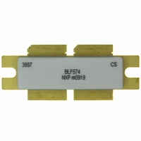
BLF574,112 NXP Semiconductors, BLF574,112 Datasheet - Page 3

BLF574,112
Manufacturer Part Number
BLF574,112
Description
TRANSISTOR RF LDMOS SOT539A
Manufacturer
NXP Semiconductors
Datasheet
1.BLF574112.pdf
(18 pages)
Specifications of BLF574,112
Package / Case
SOT539A
Transistor Type
LDMOS
Frequency
225MHz
Gain
26.5dB
Voltage - Rated
110V
Current Rating
56A
Current - Test
1A
Voltage - Test
50V
Power - Output
400W
Forward Transconductance Gfs (max / Min)
17 S
Mounting Style
SMD/SMT
Resistance Drain-source Rds (on)
0.14 Ohms
Drain-source Breakdown Voltage
110 V
Gate-source Breakdown Voltage
11 V
Continuous Drain Current
56 A
Power Dissipation
500 W
Application
HF/VHF
Channel Type
N
Channel Mode
Enhancement
Drain Source Voltage (max)
110V
Output Power (max)
600W
Power Gain (typ)@vds
26.5@50VdB
Frequency (max)
500MHz
Package Type
LDMOST
Pin Count
5
Forward Transconductance (typ)
17S
Drain Source Resistance (max)
90(Typ)@6Vmohm
Input Capacitance (typ)@vds
300@50VpF
Output Capacitance (typ)@vds
72@50VpF
Reverse Capacitance (typ)
1.5@50VpF
Operating Temp Range
-65C to 225C
Drain Efficiency (typ)
70%
Mounting
Screw
Mode Of Operation
CW
Number Of Elements
2
Vswr (max)
13
Screening Level
Military
Lead Free Status / RoHS Status
Lead free / RoHS Compliant
Noise Figure
-
Lead Free Status / Rohs Status
Lead free / RoHS Compliant
Other names
568-4736
934061965112
934061965112
NXP Semiconductors
6. Characteristics
BLF574_2
Product data sheet
Table 6.
T
Table 7.
Mode of operation: CW; f = 225 MHz; RF performance at V
T
Symbol Parameter
V
V
V
I
I
I
g
R
C
C
C
Symbol Parameter
G
RL
DSS
DSX
GSS
j
case
fs
D
(BR)DSS
GS(th)
GSq
DS(on)
rs
iss
oss
p
= 25 C; per section unless otherwise specified.
in
= 25 C; unless otherwise specified; in a class-AB production test circuit.
power gain
input return loss
drain efficiency
drain-source breakdown voltage V
gate-source threshold voltage
gate-source quiescent voltage
drain leakage current
drain cut-off current
gate leakage current
forward transconductance
drain-source on-state resistance V
feedback capacitance
input capacitance
output capacitance
DC characteristics
RF characteristics
Rev. 02 — 24 February 2009
Conditions
V
V
V
V
V
V
V
I
V
f = 1 MHz
V
f = 1 MHz
V
f = 1 MHz
Conditions
P
P
P
D
GS
DS
DS
GS
GS
DS
GS
DS
GS
GS
GS
GS
L
L
L
= 8.33 A
= 400 W
= 400 W
= 400 W
= 10 V; I
= 50 V; I
= 10 V
= 10 V; I
= 0 V; I
= 0 V; V
= V
= 11 V; V
= V
= 0 V; V
= 0 V; V
= 0 V; V
GS(th)
GS(th)
D
DS
DS
DS
DS
D
D
D
= 2.5 mA
+ 3.75 V;
+ 3.75 V;
DS
DS
HF / VHF power LDMOS transistor
= 250 mA
= 500 mA
= 12.5 A
= 50 V
= 50 V;
= 50 V;
= 50 V;
= 50 V; I
= 0 V
Dq
= 1000 mA for total device;
Min Typ Max Unit
110 -
1.25 1.7
1.35 1.85 2.35 V
-
29
-
-
-
-
-
-
Min Typ Max Unit
25
13
66
© NXP B.V. 2009. All rights reserved.
BLF574
-
37.5 -
-
17
0.14 -
1.5
204 -
72
26.5 28
20
70
-
2.25 V
2.8
280 nA
-
-
-
-
-
3 of 18
V
A
S
pF
pF
pF
dB
dB
%
A


