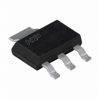
BFG97,115 NXP Semiconductors, BFG97,115 Datasheet - Page 2

BFG97,115
Manufacturer Part Number
BFG97,115
Description
TRANS NPN 15V 5.5GHZ SOT223
Manufacturer
NXP Semiconductors
Datasheet
1.BFG97115.pdf
(16 pages)
Specifications of BFG97,115
Package / Case
SOT-223 (3 leads + Tab), SC-73, TO-261
Transistor Type
NPN
Voltage - Collector Emitter Breakdown (max)
15V
Frequency - Transition
5.5GHz
Power - Max
1W
Dc Current Gain (hfe) (min) @ Ic, Vce
25 @ 70mA, 10V
Current - Collector (ic) (max)
100mA
Mounting Type
Surface Mount
Dc Current Gain Hfe Max
25 @ 70mA @ 10V
Mounting Style
SMD/SMT
Configuration
Single Dual Emitter
Transistor Polarity
NPN
Maximum Operating Frequency
5500 MHz (Typ)
Collector- Emitter Voltage Vceo Max
15 V
Emitter- Base Voltage Vebo
3 V
Continuous Collector Current
0.1 A
Power Dissipation
1000 mW
Maximum Operating Temperature
+ 175 C
Number Of Elements
1
Collector-emitter Voltage
15V
Collector-base Voltage
20V
Emitter-base Voltage
3V
Collector Current (dc) (max)
100mA
Dc Current Gain (min)
25
Frequency (max)
5.5GHz
Operating Temp Range
-65C to 175C
Operating Temperature Classification
Military
Mounting
Surface Mount
Pin Count
3 +Tab
Package Type
SOT-223
Lead Free Status / RoHS Status
Lead free / RoHS Compliant
Gain
-
Noise Figure (db Typ @ F)
-
Lead Free Status / Rohs Status
Lead free / RoHS Compliant
Other names
568-1986-2
933919920115
BFG97 T/R
933919920115
BFG97 T/R
NXP Semiconductors
DESCRIPTION
NPN planar epitaxial transistor
mounted in a plastic SOT223
envelope.
It features excellent output voltage
capabilities, and is primarily intended
for use in MATV applications.
PNP complement is the BFG31.
QUICK REFERENCE DATA
LIMITING VALUES
In accordance with the Absolute Maximum System (IEC 134).
Note
1. T
September 1995
V
V
I
P
h
f
G
V
V
V
V
I
P
T
T
SYMBOL
C
T
C
SYMBOL
FE
stg
j
CBO
CEO
tot
o
CBO
CEO
EBO
tot
NPN 5 GHz wideband transistor
UM
s
is the temperature at the soldering point of the collector tab.
collector-base voltage
collector-emitter voltage
DC collector current
total power dissipation
DC current gain
transition frequency
maximum unilateral power gain
output voltage
collector-base voltage
collector-emitter voltage
emitter-base voltage
DC collector current
total power dissipation
storage temperature
junction temperature
PARAMETER
PARAMETER
PINNING
PIN
1
2
3
4
open emitter
open base
up to T
I
I
f = 500 MHz; T
I
f = 500 MHz; T
I
f = 800 MHz; T
I
d
f
C
C
C
C
C
(pqr)
im =
emitter
base
emitter
collector
= 70 mA; V
= 70 mA; V
= 70 mA; V
= 70 mA; V
= 70 mA; V
open emitter
open base
open collector
up to T
60 dB; R
DESCRIPTION
s
= 793.25 MHz; T
= 125 C (note 1)
2
s
CONDITIONS
= 125 C (note 1)
CE
CE
CE
CE
CE
L
CONDITIONS
amb
amb
amb
= 75 ;
= 10 V; T
= 10 V;
= 10 V;
= 10 V;
= 10 V;
= 25 C
= 25 C
= 25 C
amb
j
= 25 C
= 25 C
age
Top view
25
MIN.
65
Fig.1 SOT223.
1
MIN.
Product specification
80
5.5
16
12
700
TYP.
20
15
3
100
1
150
175
2
MAX.
20
15
100
1
MAX.
BFG97
4
MSB002 - 1
V
V
V
mA
W
C
C
3
UNIT
V
V
mA
W
GHz
dB
dB
mV
UNIT


