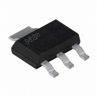
BFG94,115 NXP Semiconductors, BFG94,115 Datasheet - Page 7

BFG94,115
Manufacturer Part Number
BFG94,115
Description
TRANS NPN 10V 60MA SOT223
Manufacturer
NXP Semiconductors
Datasheet
1.BFG94115.pdf
(13 pages)
Specifications of BFG94,115
Package / Case
SOT-223 (3 leads + Tab), SC-73, TO-261
Transistor Type
NPN
Voltage - Collector Emitter Breakdown (max)
12V
Frequency - Transition
6GHz
Noise Figure (db Typ @ F)
2.7dB ~ 3dB @ 500MHz ~ 1GHz
Power - Max
700mW
Dc Current Gain (hfe) (min) @ Ic, Vce
45 @ 30mA, 5V
Current - Collector (ic) (max)
60mA
Mounting Type
Surface Mount
Dc Current Gain Hfe Max
45
Mounting Style
SMD/SMT
Configuration
Single
Transistor Polarity
NPN
Maximum Operating Frequency
4000 MHz
Collector- Emitter Voltage Vceo Max
12 V
Emitter- Base Voltage Vebo
2 V
Continuous Collector Current
0.06 A
Power Dissipation
700 mW
Maximum Operating Temperature
+ 175 C
Lead Free Status / RoHS Status
Lead free / RoHS Compliant
Gain
-
Lead Free Status / RoHS Status
Lead free / RoHS Compliant, Lead free / RoHS Compliant
Other names
934002270115
BFG94 T/R
BFG94 T/R
BFG94 T/R
BFG94 T/R
Philips Semiconductors
September 1995
handbook, halfpage
handbook, halfpage
NPN 6 GHz wideband transistor
G max
I
Fig.10 Maximum available stable gain as a
I
See test circuit, Fig.2
Fig.12 Second order intermodulation distortion as
(dB)
c
c
(dB)
d 2
= 20 mA; V
= 45 mA; V
20
15
10
20
40
60
80
0
5
10
10
function of frequency.
a function of collector current.
CE
CE
= 10 V; f
= 8 V.
10
(p q)
30
2
= 810 MHz.
10
50
3
f (MHz)
I
C
(mA)
MBB782
MBB794
10
70
4
7
handbook, halfpage
handbook, halfpage
V
G
G
I
See test circuit, Fig.2
Fig.13 Third order intermodulation distortion as a
c
gain
(dB)
(dB)
CE
max
UM
d 3
= 45 mA; V
Fig.11 Gain as a function of collector current.
= 8 V; f = 1 GHz.
30
20
10
= maximum unilateral power gain.
20
40
60
80
= maximum available stable gain.
0
10
0
function of collector current.
CE
= 10 V; f
10
(p q r)
30
20
= 793.25 MHz.
30
50
Product specification
G max
G UM
I
40
C
I
(mA)
C
MBB781
MBB795
(mA)
BFG94
50
70


