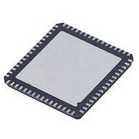
AD9548BCPZ Analog Devices Inc, AD9548BCPZ Datasheet - Page 101

AD9548BCPZ
Manufacturer Part Number
AD9548BCPZ
Description
IC CLOCK GEN/SYNCHRONIZR 88LFCSP
Manufacturer
Analog Devices Inc
Datasheet
1.AD9548BCPZ-REEL7.pdf
(112 pages)
Specifications of AD9548BCPZ
Input
*
Output
*
Frequency - Max
*
Voltage - Supply
*
Operating Temperature
*
Mounting Type
Surface Mount
Package / Case
88-LFCSP
Frequency-max
*
Clock Ic Type
Clock Synthesizer
Ic Interface Type
Serial
Frequency
1GHz
No. Of Outputs
4
No. Of Multipliers / Dividers
4
Supply Current
190mA
Lead Free Status / RoHS Status
Lead free / RoHS Compliant
Available stocks
Company
Part Number
Manufacturer
Quantity
Price
Part Number:
AD9548BCPZ
Manufacturer:
ADI/亚德诺
Quantity:
20 000
Company:
Part Number:
AD9548BCPZ-SMD7
Manufacturer:
SHARP
Quantity:
392
EEPROM STORAGE SEQUENCE (REGISTER 0E10 TO REGISTER 0E3F)
The default settings of Register 0E10 to Register 0E33 embody a sample scratch pad instruction sequence. The following is a description
of the register defaults under the assumption that the controller has been instructed to carry out an EEPROM storage sequence.
Table 141. EEPROM Storage Sequence for System Clock Settings
Address
0E10
0E11
0E12
0E13
Table 142. EEPROM Storage Sequence for System Clock Calibration
Address
0E14
Table 143. EEPROM Storage Sequence for General Configuration Settings
Address
0E15
0E16
0E17
Table 144. EEPROM Storage Sequence for DPLL Settings
Address
0E18
0E19
0E1A
Bits
[7:0]
[7:0]
[7:0]
[7:0]
Bits
[7:0]
Bits
[7:0]
[7:0]
[7:0]
Bits
[7:0]
[7:0]
[7:0]
Bit Name
System clock
System clock
I/O update
Bit Name
SYSCLK calibrate
Bit Name
General
General
Bit Name
DPLL
DPLL
Description
The default value of this register is 0x08, which the controller interprets as a data
instruction. Its decimal value is 8, which tells the controller to transfer nine bytes of
data (8 + 1) beginning at the address specified by the next two bytes. The
controller stores 0x08 in the EEPROM and increments the EEPROM address pointer.
The default value of these two registers is 0x0100. Note that Register 0E11 and
Register 0E12 are the most significant and least significant bytes of the target
address, respectively. Because the previous register contains a data instruction,
these two registers define a starting address (in this case, 0x0100). The controller
stores 0x0100 in the EEPROM and increments the EEPROM pointer by 2. It then
transfers nine bytes from the register map (beginning at Address 0x0100) to the
EEPROM and increments the EEPROM address pointer by 10 (nine data bytes and
one checksum byte). The nine bytes transferred correspond to the system clock
parameters in the register map.
The default value of this register is 0x80, which the controller interprets as an I/O
update instruction. The controller stores 0x80 in the EEPROM and increments the
EEPROM address pointer.
Description
The default value of this register is 0xA0, which the controller interprets as a
calibrate instruction. The controller stores 0xA0 in the EEPROM and increments the
EEPROM address pointer.
Description
The default value of this register is 0x14, which the controller interprets as a data
instruction. Its decimal value is 20, which tells the controller to transfer 21 bytes of
data (20 + 1) beginning at the address specified by the next two bytes. The
controller stores 0x14 in the EEPROM and increments the EEPROM address pointer.
The default value of these two registers is 0x0200. Note that Register 0E16 and
Register 0E17 are the most significant and least significant bytes of the target
address, respectively. Because the previous register contains a data instruction,
these two registers define a starting address (in this case, 0x0200). The controller
stores 0x0200 in the EEPROM and increments the EEPROM pointer by 2. It then
transfers 21 bytes from the register map (beginning at Address 0x0200) to the
EEPROM and increments the EEPROM address pointer by 22 (21 data bytes and
one checksum byte). The 21 bytes transferred correspond to the general
configuration parameters in the register map.
Description
The default value of this register is 0x1B, which the controller interprets as a data
instruction. Its decimal value is 27, which tells the controller to transfer 28 bytes
of data (27 + 1) beginning at the address specified by the next two bytes. The
controller stores 0x1B in the EEPROM and increments the EEPROM address pointer.
The default value of these two registers is 0x0300. Note that Register 0E19 and
Register 0E1A are the most significant and least significant bytes of the target
address, respectively. Because the previous register contains a data instruction,
these two registers define a starting address (in this case, 0x0300). The controller
stores 0x0300 in the EEPROM and increments the EEPROM pointer by 2. It then
transfers 28 bytes from the register map (beginning at Address 0x0300) to the
EEPROM and increments the EEPROM address pointer by 29 (28 data bytes and
one checksum byte). The
28 bytes transferred correspond to the DPLL parameters in the register map.
Rev. A | Page 101 of 112
AD9548


