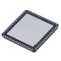
AD9548BCPZ Analog Devices Inc, AD9548BCPZ Datasheet - Page 37

AD9548BCPZ
Manufacturer Part Number
AD9548BCPZ
Description
IC CLOCK GEN/SYNCHRONIZR 88LFCSP
Manufacturer
Analog Devices Inc
Datasheet
1.AD9548BCPZ-REEL7.pdf
(112 pages)
Specifications of AD9548BCPZ
Input
*
Output
*
Frequency - Max
*
Voltage - Supply
*
Operating Temperature
*
Mounting Type
Surface Mount
Package / Case
88-LFCSP
Frequency-max
*
Clock Ic Type
Clock Synthesizer
Ic Interface Type
Serial
Frequency
1GHz
No. Of Outputs
4
No. Of Multipliers / Dividers
4
Supply Current
190mA
Lead Free Status / RoHS Status
Lead free / RoHS Compliant
Available stocks
Company
Part Number
Manufacturer
Quantity
Price
Part Number:
AD9548BCPZ
Manufacturer:
ADI/亚德诺
Quantity:
20 000
Company:
Part Number:
AD9548BCPZ-SMD7
Manufacturer:
SHARP
Quantity:
392
The worst-case scenario is maximum f
(62.5 MHz), which yields Δf
in 10 trillion.
Recovery from Holdover
When in holdover and a valid reference becomes available, the
device exits holdover operation. The loop state machine restores
the DPLL to closed-loop operation, locks to the selected reference,
and sequences the recovery of all the loop parameters based on
the profile settings for the active reference.
Note that, if the user holdover bit (Register 0A01, Bit 6) is set,
the device does not automatically exit holdover when a valid
reference is available. However, automatic recovery can occur
after clearing the user holdover bit.
SYSTEM CLOCK INPUTS
Functional Description
The system clock circuit provides a low jitter, stable, high frequency
clock for use by the rest of the chip. The user has the option of
directly driving the SYSCLKx inputs with a high frequency
clock source at the desired system clock rate. Alternatively, the
SYSCLKx input can be configured to operate in conjunction
with the internal SYSCLK PLL. The SYSCLK PLL can synthesize
the system clock by means of a crystal resonator connected
across the SYSCLKx input pins or by means of direct application
of a low frequency clock source.
The SYSCLKx inputs are internally biased to a dc level of ~1 V. Take
care to ensure that any external connections do not disturb the dc
bias because this may significantly degrade performance. Generally,
the recommendation is that the SYSCLKx inputs be ac-coupled
to the signal source (except when using a crystal resonator).
Low Loop Bandwidth Applications Using a TCXO/OCXO
For many applications, the use of a crystal oscillator is a cost-
effective and simple choice. The stability is good enough to support
loop bandwidths down to 50 Hz, and the holdover performance
is good enough for all except the most demanding applications.
SYSCLKN
SYSCLKP
52
53
O
/f
LF
HF
XTAL
O
= 2.8 × 10
S
(1 GHz) and minimum f
−14
, less than one part
÷M
2×
Figure 45. System Clock Block Diagram
Rev. A | Page 37 of 112
O
DETECT
CHARGE
LOCK
PUMP
PFD
AND
In cases where Stratum 2 or Stratum 3 holdover performance is
needed, or in cases where the loop bandwidth must be <50 Hz,
the user must use either a TCXO or OCXO. The user should
choose a TCXO/OCXO with a high output frequency and
CMOS output to achieve the best performance.
When interfacing the TCXO/OCXO, a voltage divider on the
output should be used to reduce the voltage swing to 1 V p-p,
and that signal should be ac-coupled to the SYSCLKP pin. The
SYSCLKN pin can be bypassed to ground with a 0.01 μF capacitor.
Choosing the System Clock Oscillator Frequency
The best performance of the AD9548 is achieved when the system
clock is not an integer multiple of the DDS output frequency.
As an example, using a 19.44 MHz oscillator for the system
clock in a 156.25 MHz Ethernet application yields better
performance than a 25 MHz oscillator.
Another good system clock choice for many communications
applications is a 49.152 MHz crystal used in IEEE 1394 (FireWire)
because nearly all output frequencies are not integer related to
this frequency, and the crystal is readily available.
System Clock Details
A block diagram of the system clock appears in Figure 45. The
signal at the SYSCLKx input pins becomes the internally buffered
DAC sampling clock (f
Note that both the LF and XTAL paths require the use of the
SYSCLK PLL (see the SYSCLK PLL Multiplier section).
The main purpose of the HF path is to allow the direct use of a high
frequency (500 MHz to 1 GHz) external clock source for clocking
the AD9548. This path is optimized for high frequency and low
noise floor. Note that the HF input also provides a path to SYSCLK
PLL (see the SYSCLK PLL Multiplier section), which includes
an input divider (M) programmable for divide-by -1, -2, -4, or -8.
The purpose of the divider is to limit the frequency at the input
to the PLL to less than 150 MHz (the maximum PFD rate).
SYSCLK_VREG
High frequency direct (HF)
Low frequency synthesized (LF)
Crystal resonator synthesized (XTAL)
48
FILTER
LOOP
÷N
SYSCLK_LF
CALIBRATION
49
S
) via one of three paths.
VCO
SYSTEM
CLOCK
AD9548


