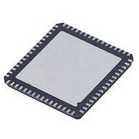
AD9548BCPZ Analog Devices Inc, AD9548BCPZ Datasheet - Page 42

AD9548BCPZ
Manufacturer Part Number
AD9548BCPZ
Description
IC CLOCK GEN/SYNCHRONIZR 88LFCSP
Manufacturer
Analog Devices Inc
Datasheet
1.AD9548BCPZ-REEL7.pdf
(112 pages)
Specifications of AD9548BCPZ
Input
*
Output
*
Frequency - Max
*
Voltage - Supply
*
Operating Temperature
*
Mounting Type
Surface Mount
Package / Case
88-LFCSP
Frequency-max
*
Clock Ic Type
Clock Synthesizer
Ic Interface Type
Serial
Frequency
1GHz
No. Of Outputs
4
No. Of Multipliers / Dividers
4
Supply Current
190mA
Lead Free Status / RoHS Status
Lead free / RoHS Compliant
Available stocks
Company
Part Number
Manufacturer
Quantity
Price
Part Number:
AD9548BCPZ
Manufacturer:
ADI/亚德诺
Quantity:
20 000
Company:
Part Number:
AD9548BCPZ-SMD7
Manufacturer:
SHARP
Quantity:
392
AD9548
Active Reference Synchronization (Zero Delay)
Active reference synchronization is the term applied to the case
when sync source = 01 (Register 0402, Bits[5:4]). Referring to
Figure 48, this means that the active reference sync path is
active because Bit 4 = 1, enabling the lower AND gate and
disabling the upper AND gate. The edge detector in the active
reference sync block monitors the rising edges of the active
reference (the mux selects the active reference automatically).
The edge detector is armed via the primary synchronization
signal, which is one of the four inputs to the OR gate (typically
the direct sync source). As soon as the edge detector is armed,
its output goes high, which stalls the output dividers in the
clock distribution block. Furthermore, once armed, a rising
edge from the active reference forces the output of the edge
detector low. This restarts the output dividers, thereby
synchronizing the clock distribution block.
MULTIFUNCTION PIN
(REGISTER 0A02[1])
AUTOMATIC SYNC
(REGISTER 0403)
SYNC SOURCE
EEPROM SYNC
DIRECT SYNC
SOURCE
SOURCE
SOURCE
SYNCHRONIZATION
PRIMARY
SIGNAL
FEEDBACK
DETECT
EDGE
DPLL
EDGE
Figure 48. Output Synchronization Block Diagram
DPLL EDGE SYNC
DIRECT SYNC
ARM
SYSCLK/4
DETECT
EDGE
Rev. A | Page 42 of 112
REGISTER
0402[4]
REGISTER
The term zero delay applies because it provides a means to edge
align the output signal with the active input reference signal.
Typically, zero-delay architectures use the output signal in the
feedback loop of a PLL to track input/output edge alignment.
Active reference synchronization, however, operates open loop.
That is, synchronization of the output via the distribution
synchronization logic occurs on a single edge of the active
reference.
The fact that an active reference edge triggers the falling edge of
the synchronization pulse means that the falling edge is
asynchronous to the signal that clocks the distribution output
dividers (CLKINx). Therefore, the output clock distribution
logic reclocks the internal synchronization pulse to synchronize
it with the CLKINx signal. This means that the output dividers
restart after a deterministic delay associated with the reclocking
circuitry. This deterministic delay has two components. The
first deterministic delay component is four or five periods of the
CLKINx signal. The one period uncertainty is due to the
unknown position of the asynchronous reference clock edge
relative to the CLKINx signal. The second deterministic delay
component is one output period of the distribution divider.
0402[5]
REF AA
REF DD
ACTIVE REFERENCE SYNC
REF A
REF D
0
1
ARM
RESET
DETECT
EDGE
TO MULTIFUNCTION
PIN STATUS LOGIC
TO CLOCK
DISTRIBUTION
SYNCHRONIZATION
CONTROL
DIVIDERS
STALL
SYNC OUTPUT
DISTRIBUTION


