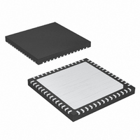
MAX19711ETN+T Maxim Integrated Products, MAX19711ETN+T Datasheet - Page 18

MAX19711ETN+T
Manufacturer Part Number
MAX19711ETN+T
Description
IC ANLG FRNT END 56-TQFN
Manufacturer
Maxim Integrated Products
Datasheet
1.MAX19711ETN.pdf
(36 pages)
Specifications of MAX19711ETN+T
Number Of Bits
10
Number Of Channels
2
Power (watts)
37.5mW
Voltage - Supply, Analog
3V
Voltage - Supply, Digital
3V
Package / Case
56-TQFN Exposed Pad
Lead Free Status / RoHS Status
Lead free / RoHS Compliant
tial input stage with ≥ 70kΩ input impedance. This simpli-
fies the analog interface between RF quadrature upcon-
verters and the MAX19711. Many RF upconverters
require a 0.86V to 1.36V common-mode bias. The
MAX19711 common-mode DC bias eliminates discrete
level-setting resistors and code-generated level shifting
while preserving the full dynamic range of each Tx DAC.
The Tx DAC differential analog outputs cannot be
used in single-ended mode because of the internally
generated common-mode DC level. Table 2 shows the
10-Bit, 11Msps, Full-Duplex
Analog Front-End
18
Figure 3. Rx ADC System Timing Diagram
Table 2. Tx Path Output Voltage vs. Input Codes
(Internal Reference Mode V
Full Scale and V
DIFFERENTIAL OUTPUT VOLTAGE (V)
______________________________________________________________________________________
QA
D0–D9
CLK
t
DOQ
IA
(
(
(
V
V
V
(
(
(
(
V
FS
FS
FS
V
V
V
FS
FS
FS
FS
)
)
)
)
)
)
)
−
−
−
V
V
V
V
V
V
V
REFDAC
FS
REFDAC
REFDAC
REFDAC
REFDAC
REFDAC
REFDAC
t
1024
1024
1024
CL
1024
D0Q
1024
1024
1024
= 500 for 1V
t
CLK
t
×
CH
×
×
×
×
×
×
D1I
1023
1023
1023
1023
1023
1023
1023
1023
1023
1021
1021
3
1
1
REFDAC
t
DOI
D1Q
P-P
Full Scale)
= 1.024V, External Reference Mode V
D2I
OFFSET BINARY (DA0–DA9)
D2Q
5.5 CLOCK-CYCLE LATENCY (CHQ)
5 CLOCK-CYCLE LATENCY (CHI)
11 1111 1111
11 1111 1110
10 0000 0001
10 0000 0000
01 1111 1111
00 0000 0001
00 0000 0000
D3I
D3Q
Tx path output voltage vs. input codes. Table 11 shows
the selection of DC common-mode levels. See Figure 5
for an illustration of the Tx DAC analog output levels.
The buffer amplifiers also feature a programmable full-
scale output level of ±410mV or ±500mV and indepen-
dent DC offset trim on each ID–QD channel. Both features
are configured through the SPI interface. The DC offset
correction is used to optimize sideband and carrier sup-
pression in the Tx signal path (see Tables 8 and 10).
D4I
REFDAC
D4Q
= V
D5I
REFIN
INPUT DECIMAL CODE
D5Q
, V
FS
1023
1022
513
512
511
= 410 for 820mV
1
0
D6I
D6Q
P-P


