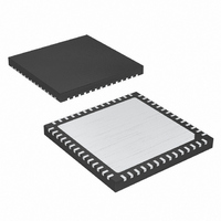
MAX19711ETN+T Maxim Integrated Products, MAX19711ETN+T Datasheet - Page 28

MAX19711ETN+T
Manufacturer Part Number
MAX19711ETN+T
Description
IC ANLG FRNT END 56-TQFN
Manufacturer
Maxim Integrated Products
Datasheet
1.MAX19711ETN.pdf
(36 pages)
Specifications of MAX19711ETN+T
Number Of Bits
10
Number Of Channels
2
Power (watts)
37.5mW
Voltage - Supply, Analog
3V
Voltage - Supply, Digital
3V
Package / Case
56-TQFN Exposed Pad
Lead Free Status / RoHS Status
Lead free / RoHS Compliant
10-Bit, 11Msps, Full-Duplex
Analog Front-End
Table 18. Auxiliary ADC Data Output Mode
the system CLK frequency supplied to the MAX19711
(see Table 17). The total conversion time (t
auxiliary ADC can be calculated as t
N
averages (see Table 16), N
Table 17), and f
DOUT is normally in a high-impedance condition. Upon
setting the auxiliary ADC start conversion bit (bit AD0),
DOUT becomes active and goes high, indicating that
the aux-ADC is busy. When the conversion cycle is
complete (including averaging), the data is placed into
an output register and DOUT goes low, indicating that
the output data is ready to be driven onto DOUT. When
bit AD10 is set (AD10 = 1), the aux-ADC enters a data
output mode where data is available at DOUT on the
next low assertion of CS/WAKE. The auxiliary ADC data
is shifted out of DOUT (MSB first) with the data transi-
tioning on the falling edge of the serial clock (SCLK).
Since a DOUT read requires 16 bits, DOUT holds the
value of the last conversion data bit for the last 6 bits (6
least significant bits) following the aux-ADC conversion
data. DOUT enters a high-impedance state when
CS/WAKE is deasserted high. When bit AD10 is cleared
(AD10 = 0), the aux-ADC data is not available on DOUT
(see Table 18).
After the aux-ADC completes a conversion, the data
result is loaded to an output register waiting to be shift-
ed out. No further conversions are possible until data is
shifted out. This means that if the first conversion com-
mand sets AD10 = 0, AD0 = 1, then it cannot be fol-
lowed by conversion commands setting AD10 = 0, AD0
= 1 or AD10 = 1, AD0 = 1. If this sequence of com-
mands is inadvertently used then DOUT is disabled. To
resume normal operation set AD0 = 0.
Table 19. Reference Modes
28
AVG
AD10
1.024V ±10%
> 0.8V x V
0
1
______________________________________________________________________________________
V
x N
REFIN
DIV
Aux-ADC Data is Not Available on DOUT (Default)
DD
Reading DOUT from the Aux-ADC
) / f
Aux-ADC Enters Data Output Mode Where
CLK
CLK
Internal Reference Mode. V
with a 0.33µF capacitor.
Buffered External Reference Mode. An external 1.024V ±10% reference voltage is applied to REFIN. V
internally generated to be V
REFIN to GND with a 0.1µF capacitor.
is the system CLK frequency.
Data is Available on DOUT
; where N
SELECTION
DIV
is the CLK divisor (see
AVG
is the number of
CONV
CONV
REF
REFIN
is internally generated to be 0.512V. Bypass REFP, REFN, and COM each
= (12 x
) of the
/ 2. Bypass REFP, REFN, and COM each with a 0.33µF capacitor. Bypass
REFERENCE MODE
The fastest method to perform sequential conversions
with the aux-ADC is by sending consecutive commands
setting AD10 = 1, AD0 = 1. With this sequence the
CS/WAKE falling edge shifts data from the previous con-
version on to DOUT and the rising edge of CS/WAKE
loads the next conversion command at DIN. Allow
enough time for each conversion to complete before
sending the next conversion command. See Figure 9 for
single and continuous conversion examples.
DIN can be written independent of DOUT state. A 16-
bit instruction at DIN updates the device configuration.
To prevent modifying internal registers while reading
data from DOUT, hold DIN at a high state (only applies
if sequential aux-ADC conversions are not executed).
This effectively writes all ones into address 1111. Since
address 1111 does not exist, no internal registers are
affected.
The MAX19711 features an internal precision 1.024V-
bandgap reference that is stable over the entire power-
supply and temperature ranges. The REFIN input
provides two modes of reference operation. The volt-
age at REFIN (V
mode (Table 19).
In internal reference mode, connect REFIN to V
V
level. COM, REFP, and REFN are low-impedance out-
puts with V
and V
and COM each with a 0.33µF capacitor. Bypass REFIN
to GND with a 0.1µF capacitor.
In buffered external reference mode, apply 1.024V
±10% at REFIN. In this mode, COM, REFP, and REFN
are low-impedance outputs with V
V
V
0.33µF capacitor. Bypass REFIN to GND with a 0.1µF
capacitor. In this mode, the Tx path full-scale output is
proportional to the external reference. For example, if
the V
scale output is also increased by 10% or ±451mV.
REF
REFP
REFIN
REFIN
is an internally generated 0.512V ±4% reference
REFN
= V
/ 4. Bypass REFP, REFN, and COM each with a
DD
COM
is increased by 10% (max), the Tx path full-
= V
/ 2 + V
DD
= V
REFIN
/ 2 - V
DD
REFIN
Reference Configurations
) sets the reference operation
/ 2, V
REF
/ 4, and V
REFP
/ 2. Bypass REFP, REFN,
= V
DD
COM
REFN
/ 2 + V
= V
= V
DD
REF
REF
DD
/ 2 -
is
DD
/ 2,
/ 2,
.


