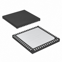
MAX19711ETN+T Maxim Integrated Products, MAX19711ETN+T Datasheet - Page 25

MAX19711ETN+T
Manufacturer Part Number
MAX19711ETN+T
Description
IC ANLG FRNT END 56-TQFN
Manufacturer
Maxim Integrated Products
Datasheet
1.MAX19711ETN.pdf
(36 pages)
Specifications of MAX19711ETN+T
Number Of Bits
10
Number Of Channels
2
Power (watts)
37.5mW
Voltage - Supply, Analog
3V
Voltage - Supply, Digital
3V
Package / Case
56-TQFN Exposed Pad
Lead Free Status / RoHS Status
Lead free / RoHS Compliant
In FAST Rx mode, the Tx path (DAC core and Tx filter) is
powered on. The Tx path outputs are set to midscale. In
this mode, the Tx DAC input bus is disconnected from
the DAC core and DA0–DA9 are internally pulled to
OV
core is fully operational.
In FAST mode, the switching time from Tx to Rx, or Rx to
Tx is minimized because the converters are on and do
not have to recover from a power-down state. In FAST
mode, the switching time from Rx to Tx is 1µs and Tx to
Rx is 0.1µs. Power consumption is higher in FAST mode
because both Tx and Rx cores are always on.
In SLOW Tx mode, the Rx ADC core is powered off and
the ADC digital outputs AD0–AD9 are tri-stated. The Tx
DAC digital bus is active and the DAC core is fully oper-
ational. In SLOW Rx mode, the Tx DAC core is powered
off. The Tx path outputs are set to 0. In SLOW Rx mode,
the Tx DAC input bus is disconnected from the DAC
core and DA0–DA9 are internally pulled to OV
Rx ADC digital bus is active and the ADC core is fully
operational. The switching times for SLOW modes are
5µs for Rx to Tx and 6.8µs for Tx to Rx.
Power consumption in SLOW Tx mode is 34.5mW, and
24.3mW in SLOW Rx mode. Power consumption in FAST
Tx mode is 42.3mW, and 41.4mW in FAST Rx mode.
The MAX19711 features an FD mode, which is ideal for
applications supporting frequency-division duplex. In
FD mode, both Rx ADC and Tx DAC, as well as their
respective digital buses, are active and the device can
receive and transmit simultaneously. Switching from FD
mode to Rx (0.1µs) or Tx (1µs) modes is fast since
the on-board converters are already powered.
Consequently, power consumption in this mode is the
maximum of all operating modes. In FD mode the
MAX19711 consumes 42.75mW.
Figure 7. Serial-Interface Timing Diagram
CS/WAKE
DD
. The Rx ADC digital bus is active and the ADC
SCLK
DIN
______________________________________________________________________________________
t
CSS
t
DS
MSB
t
DH
t
CH
t
CP
FD Mode
DD
10-Bit, 11Msps, Full-Duplex
. The
t
CL
The MAX19711 uses the SPI interface to control the
operating modes of the device including the shutdown
and wake-up functions. Once the device has been
placed in shutdown through the appropriate SPI com-
mand, the first pulse on CS/WAKE performs a wake-up
function. At the first rising edge of CS/WAKE, the
MAX19711 is forced to a preset operating mode deter-
mined by the WAKEUP-SEL register. This mode is
termed the wake-up state. If the WAKEUP-SEL register
has not been programmed, the wake-up state for the
MAX19711 is FD mode by default (Tables 6, 12). The
WAKEUP-SEL register cannot be programmed with W2
= 0, W1 = 0, and W0 = 0. If this value is inadvertently
written to the device, it is ignored and the register con-
tinues to store its previous value. Upon wake-up, the
MAX19711 enters the power mode determined by the
WAKEUP-SEL register, however, all other settings (Tx
DAC offset, Tx DAC common-mode voltage, aux-DAC
settings, aux-ADC state) are restored to their values
prior to shutdown.
The only SPI line that is monitored by the MAX19711
during shutdown is CS/WAKE. Any information transmit-
ted to the MAX19711 concurrent with the CS/WAKE
wake-up pulse is ignored.
The serial digital interface is a standard 3-wire connection
CS/WAKE, SCLK, DIN) compatible with SPI/QSPI™/
MICROWIRE/DSP interfaces. Set CS/WAKE low to enable
the serial data loading at DIN or output at DOUT.
Following a CS/WAKE high-to-low transition, data is shift-
ed synchronously, most significant bit first, on the rising
edge of the serial clock (SCLK). After 16 bits are loaded
into the serial input register, data is transferred to the
latch when CS/WAKE transitions high. CS/WAKE must
transition high for a minimum of 80ns before the next write
QSPI is a trademark of Motorola, Inc.
LSB
t
CS
Analog Front-End
t
CSW
Wake-Up Function
SPI Timing
25


