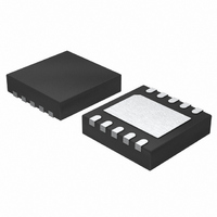
LTC2484CDD#PBF Linear Technology, LTC2484CDD#PBF Datasheet - Page 15

LTC2484CDD#PBF
Manufacturer Part Number
LTC2484CDD#PBF
Description
IC ADC 24BIT 10-DFN
Manufacturer
Linear Technology
Datasheet
1.LTC2484CDDTRPBF.pdf
(42 pages)
Specifications of LTC2484CDD#PBF
Number Of Bits
24
Sampling Rate (per Second)
6.8
Data Interface
MICROWIRE™, Serial, SPI™
Number Of Converters
1
Power Dissipation (max)
480µW
Voltage Supply Source
Single Supply
Operating Temperature
0°C ~ 70°C
Mounting Type
Surface Mount
Package / Case
10-WFDFN Exposed Pad
Number Of Elements
1
Resolution
24Bit
Architecture
Delta-Sigma
Sample Rate
0.0075KSPS
Input Polarity
Bipolar
Input Type
Voltage
Rated Input Volt
±2.75V
Differential Input
Yes
Power Supply Requirement
Single
Single Supply Voltage (typ)
3.3/5V
Single Supply Voltage (min)
2.7V
Single Supply Voltage (max)
5.5V
Dual Supply Voltage (typ)
Not RequiredV
Dual Supply Voltage (min)
Not RequiredV
Dual Supply Voltage (max)
Not RequiredV
Integral Nonlinearity Error
10ppm of Vref
Operating Temp Range
0C to 70C
Operating Temperature Classification
Commercial
Mounting
Surface Mount
Pin Count
10
Package Type
DFN EP
Input Signal Type
Differential
Lead Free Status / RoHS Status
Lead free / RoHS Compliant
Available stocks
Company
Part Number
Manufacturer
Quantity
Price
APPLICATIONS INFORMATION
Several applications leveraging this feature are presented
in more detail in the applications section. While operating
in this mode, the speed is set to normal independent of
control bit SPD.
Rejection Mode (FA, FB)
The LTC2484 includes a high accuracy on-chip oscilla-
tor with no required external components. Coupled with
a 4th order digital lowpass fi lter, the LTC2484 rejects
line frequency noise. In the default mode, the LTC2484
simultaneously rejects 50Hz and 60Hz by at least 87dB.
The LTC2484 can also be confi gured to selectively reject
50Hz or 60Hz to better than 110dB.
Speed Mode (SPD)
The LTC2484 continuously performs offset calibrations.
Every conversion cycle, two conversions are automatically
performed (default) and the results combined. This result is
free from offset and drift. In applications where the offset
is not critical, the autocalibration feature can be disabled
with the benefi t of twice the output rate.
Linearity, full-scale accuracy, full-scale drift are identical
for both 2x and 1x speed modes. In both the 1x and 2x
speed there is no latency. This enables input steps or
multiplexer channel changes to settle in a single conver-
sion cycle easing system overhead and increasing the
effective conversion rate.
Output Data Format
The LTC2484 serial output data stream is 32 bits long. The
fi rst 3 bits represent status information indicating the sign
and conversion state. The next 24 bits are the conversion
result, MSB fi rst. The remaining 5 bits are sub LSBs below
the 24-bit level. The third and fourth bit together are also
used to indicate an underrange condition (the differential
input voltage is below –FS) or an overrange condition (the
differential input voltage is above +FS).
CS may be pulled HIGH prior to outputting all 32 bits,
aborting the data out transfer and initiating a new
conversion.
Bit 31 (fi rst output bit) is the end of conversion (EOC)
indicator. This bit is available at the SDO pin during the
conversion and sleep states whenever the CS pin is LOW.
This bit is HIGH during the conversion and goes LOW when
the conversion is complete.
Bit 30 (second output bit) is a dummy bit (DMY) and is
always LOW.
Bit 29 (third output bit) is the conversion result sign
indicator (SIG). If V
this bit is LOW.
Bit 28 (fourth output bit) is the most signifi cant bit (MSB) of
the result. This bit in conjunction with bit 29 also provides
the underrange or overrange indication. If both bit 29 and
bit 28 are HIGH, the differential input voltage is above +FS.
If both bit 29 and bit 28 are LOW, the differential input
voltage is below –FS.
The function of these bits is summarized in Table 2.
Table 2. LTC2484 Status Bits
INPUT RANGE
V
0V ≤ V
–0.5 • V
V
Bits 28-5 are the 24-bit conversion result MSB fi rst.
Bits 4–0 are sub LSBs below the 24-bit level. Bits 4–0
may be included in averaging or discarded without loss
of resolution.
Data is shifted out of the SDO pin under control of the
serial clock (SCK) (see Figure 2). Whenever CS is HIGH,
SDO remains high impedance and any externally gener-
ated SCK clock pulses are ignored by the internal data
out shift register.
In order to shift the conversion result out of the device,
CS must fi rst be driven LOW. EOC is seen at the SDO pin
of the device once CS is pulled LOW. EOC changes in real
time from HIGH to LOW at the completion of a conversion.
This signal may be used as an interrupt for an external
microcontroller. Bit 31 (EOC) can be captured on the fi rst
rising edge of SCK. Bit 30 is shifted out of the device on
the fi rst falling edge of SCK. The fi nal data bit (bit 0) is
shifted out on the falling edge of the 31st SCK and may
be latched on the rising edge of the 32nd SCK pulse. On
the falling edge of the 32nd SCK pulse, SDO goes HIGH
IN
IN
≥ 0.5 • V
< –0.5 • V
IN
REF
< 0.5 • V
≤ V
REF
REF
IN
REF
< 0V
IN
is >0, this bit is HIGH. If V
BIT 31
EOC
0
0
0
0
BIT 30
DMY
0
0
0
0
LTC2484
BIT 29
SIG
1/0
1
0
0
IN
15
BIT 28
MSB
is <0,
1
0
1
0
2484fc


