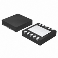
LTC2484CDD#PBF Linear Technology, LTC2484CDD#PBF Datasheet - Page 30

LTC2484CDD#PBF
Manufacturer Part Number
LTC2484CDD#PBF
Description
IC ADC 24BIT 10-DFN
Manufacturer
Linear Technology
Datasheet
1.LTC2484CDDTRPBF.pdf
(42 pages)
Specifications of LTC2484CDD#PBF
Number Of Bits
24
Sampling Rate (per Second)
6.8
Data Interface
MICROWIRE™, Serial, SPI™
Number Of Converters
1
Power Dissipation (max)
480µW
Voltage Supply Source
Single Supply
Operating Temperature
0°C ~ 70°C
Mounting Type
Surface Mount
Package / Case
10-WFDFN Exposed Pad
Number Of Elements
1
Resolution
24Bit
Architecture
Delta-Sigma
Sample Rate
0.0075KSPS
Input Polarity
Bipolar
Input Type
Voltage
Rated Input Volt
±2.75V
Differential Input
Yes
Power Supply Requirement
Single
Single Supply Voltage (typ)
3.3/5V
Single Supply Voltage (min)
2.7V
Single Supply Voltage (max)
5.5V
Dual Supply Voltage (typ)
Not RequiredV
Dual Supply Voltage (min)
Not RequiredV
Dual Supply Voltage (max)
Not RequiredV
Integral Nonlinearity Error
10ppm of Vref
Operating Temp Range
0C to 70C
Operating Temperature Classification
Commercial
Mounting
Surface Mount
Pin Count
10
Package Type
DFN EP
Input Signal Type
Differential
Lead Free Status / RoHS Status
Lead free / RoHS Compliant
Available stocks
Company
Part Number
Manufacturer
Quantity
Price
LTC2484
APPLICATIONS INFORMATION
V
tional INL error. Figure 19 shows the typical INL error due
to the source resistance driving the V
C
source impedance driving the V
In applications where the reference and input common
mode voltages are different, extra errors are introduced.
For every 1V of the reference and input common mode
voltage difference (V
each Ohm of reference source resistance introduces an
extra (V
which is 0.074ppm when using internal oscillator and 60Hz
mode. When using internal oscillator and 50Hz/60Hz mode,
the extra full-scale gain error is 0.067ppm. When using
internal oscillator and 50Hz mode, the extra gain error is
0.061ppm. If an external clock is used, the corresponding
extra gain error is 0.24 • 10
The magnitude of the dynamic reference current depends
upon the size of the very stable internal sampling capacitors
and upon the accuracy of the converter sampling clock. The
accuracy of the internal clock over the entire temperature
and power supply range is typically better than 0.5%. Such
a specifi cation can also be easily achieved by an external
clock. When relatively stable resistors (50ppm/°C) are
used for the external source impedance seen by V
and GND, the expected drift of the dynamic current gain
error will be insignifi cant (about 1% of its value over the
30
REF
REF
values are used. The user is advised to minimize the
translates into about 2.18 • 10
Figure 19. INL vs Differential Input Voltage and
Reference Source Resistance for C
REFCM
–10
10
–2
–4
–6
–8
8
6
4
2
0
–0.5
V
V
V
T
C
– V
A
CC
REF
IN(CM)
REF
= 25°C
= 5V
INCM
= 5V
= 10μF
–0.3
= 2.5V
REFCM
)/(V
–0.1
V
IN
REF
/V
– V
–6
REF
• R
0.1
• f
(V)
INCM
REF
EOSC
EQ
R = 500Ω
R = 100Ω
) full-scale gain error,
R = 1k
) and a 5V reference,
–6
pin.
0.3
ppm.
REF
REF
• f
2484 F19
EOSC
pin when large
> 1μF
0.5
ppm addi-
REF
+
entire temperature and voltage range). Even for the most
stringent applications a one-time calibration operation
may be suffi cient.
In addition to the reference sampling charge, the refer-
ence pins ESD protection diodes have a temperature
dependent leakage current. This leakage current, nominally
1nA (±10nA max), results in a small gain error. A 100Ω
source resistance will create a 0.05μV typical and 0.5μV
maximum full-scale error.
Output Data Rate
When using its internal oscillator, the LTC2484 produces
up to 7.5 samples per second (sps) with a notch frequency
of 60Hz, 6.25sps with a notch frequency of 50Hz and
6.8ps with the 50Hz/60Hz rejection mode. The actual
output data rate will depend upon the length of the sleep
and data output phases which are controlled by the user
and which can be made insignifi cantly short. When oper-
ated with an external conversion clock (f
an external oscillator), the LTC2484 output data rate can
be increased as desired. The duration of the conversion
phase is 41036/f
behaves as if the internal oscillator is used and the notch
is set at 60Hz.
An increase in f
late into a proportional increase in the maximum output
data rate. The increase in output rate is nevertheless
accompanied by three potential effects, which must be
carefully considered.
First, a change in f
in the internal notch position and in a reduction of the
converter differential mode rejection at the power line
frequency. In many applications, the subsequent per-
formance degradation can be substantially reduced by
relying upon the LTC2484’s exceptional common mode
rejection and by carefully eliminating common mode to
differential mode conversion sources in the input circuit.
The user should avoid single-ended input fi lters and should
maintain a very high degree of matching and symmetry
in the circuits driving the IN
Second, the increase in clock frequency will increase
proportionally the amount of sampling charge transferred
EOSC
EOSC
EOSC
over the nominal 307.2kHz will trans-
. If f
will result in a proportional change
EOSC
+
and IN
= 307.2kHz, the converter
–
pins.
O
connected to
2484fc


