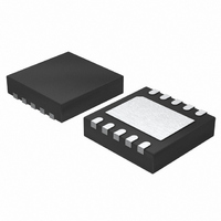
LTC2484CDD#PBF Linear Technology, LTC2484CDD#PBF Datasheet - Page 16

LTC2484CDD#PBF
Manufacturer Part Number
LTC2484CDD#PBF
Description
IC ADC 24BIT 10-DFN
Manufacturer
Linear Technology
Datasheet
1.LTC2484CDDTRPBF.pdf
(42 pages)
Specifications of LTC2484CDD#PBF
Number Of Bits
24
Sampling Rate (per Second)
6.8
Data Interface
MICROWIRE™, Serial, SPI™
Number Of Converters
1
Power Dissipation (max)
480µW
Voltage Supply Source
Single Supply
Operating Temperature
0°C ~ 70°C
Mounting Type
Surface Mount
Package / Case
10-WFDFN Exposed Pad
Number Of Elements
1
Resolution
24Bit
Architecture
Delta-Sigma
Sample Rate
0.0075KSPS
Input Polarity
Bipolar
Input Type
Voltage
Rated Input Volt
±2.75V
Differential Input
Yes
Power Supply Requirement
Single
Single Supply Voltage (typ)
3.3/5V
Single Supply Voltage (min)
2.7V
Single Supply Voltage (max)
5.5V
Dual Supply Voltage (typ)
Not RequiredV
Dual Supply Voltage (min)
Not RequiredV
Dual Supply Voltage (max)
Not RequiredV
Integral Nonlinearity Error
10ppm of Vref
Operating Temp Range
0C to 70C
Operating Temperature Classification
Commercial
Mounting
Surface Mount
Pin Count
10
Package Type
DFN EP
Input Signal Type
Differential
Lead Free Status / RoHS Status
Lead free / RoHS Compliant
Available stocks
Company
Part Number
Manufacturer
Quantity
Price
LTC2484
APPLICATIONS INFORMATION
indicating the initiation of a new conversion cycle. This
bit serves as EOC (bit 31) for the next conversion cycle.
Table 3 summarizes the output data format.
As long as the voltage on the IN+ and IN– pins is maintained
within the –0.3V to (V
operating range, a conversion result is generated for any
differential input voltage V
+FS = 0.5 • V
than +FS, the conversion result is clamped to the value
corresponding to the +FS + 1LSB. For differential input
voltages below –FS, the conversion result is clamped to
the value corresponding to –FS – 1LSB.
Conversion Clock
A major advantage the delta-sigma converter offers over
conventional type converters is an on-chip digital fi lter
(commonly implemented as a SINC or Comb fi lter). For
high resolution, low frequency applications, this fi lter is
typically designed to reject line frequencies of 50Hz or 60Hz
plus their harmonics. The fi lter rejection performance is
directly related to the accuracy of the converter system
clock. The LTC2484 incorporates a highly accurate on-chip
oscillator. This eliminates the need for external frequency
setting components such as crystals or oscillators.
Frequency Rejection Selection (f
The LTC2484 internal oscillator provides better than 110dB
normal mode rejection at the line frequency and all its
16
Table 3. LTC2484 Output Data Format
DIFFERENTIAL INPUT VOLTAGE
V
V
FS** – 1LSB
0.5 • FS**
0.5 • FS** – 1LSB
0
–1LSB
–0.5 • FS**
–0.5 • FS** – 1LSB
–FS**
V
*** The sign bit changes state during the 0 output code when the device is operating in the 2× speed mode .
** The full-scale voltage FS = 0.5 • V
IN
IN
IN
* The differential input voltage V
*
* ≥ FS**
* < –FS**
REF
. For differential input voltages greater
CC
IN
+ 0.3V) absolute maximum
from –FS = –0.5 • V
O
)
IN
BIT 31
= IN
EOC
REF
0
0
0
0
0
0
0
0
0
0
.
+
– IN
BIT 30
DMY
–
.
0
0
0
0
0
0
0
0
0
0
REF
BIT 29
1/0***
SIG
to
1
1
1
1
0
0
0
0
0
harmonics (up to the 255th) for 50Hz ±2% or 60Hz ±2%,
or better than 87dB normal mode rejection from 48Hz to
62.4Hz. The rejection mode is selected by writing to the
on-chip confi guration register and the default mode at
POR is simultaneous 50Hz/60Hz rejection.
When a fundamental rejection frequency different from
50Hz or 60Hz is required or when the converter must be
synchronized with an outside source, the LTC2484 can
operate with an external conversion clock. The converter
automatically detects the presence of an external clock
signal at the f
The frequency f
10kHz to be detected. The external clock signal duty cycle
is not signifi cant as long as the minimum and maximum
specifi cations for the high and low periods t
are observed.
While operating with an external conversion clock of a
frequency f
normal mode rejection in a frequency range of f
±4% and its harmonics. The normal mode rejection as a
function of the input frequency deviation from f
is shown in Figure 3.
Whenever an external clock is not present at the f
the converter automatically activates its internal oscilla-
tor and enters the internal conversion clock mode. The
LTC2484 operation will not be disturbed if the change of
conversion clock source occurs during the sleep state
or during the data output state while the converter uses
BIT 28
MSB
1
0
0
0
0
1
1
1
1
0
BIT 27
0
1
1
0
0
1
1
0
0
1
EOSC
O
EOSC
, the LTC2484 provides better than 110dB
BIT 26
pin and turns off the internal oscillator.
0
1
0
1
0
1
0
1
0
1
of the external signal must be at least
BIT 25
0
1
0
1
0
1
0
1
0
1
…
…
…
…
…
…
…
…
…
…
…
BIT 0
0
1
0
1
0
1
0
1
0
1
HEO
EOSC
EOSC
and t
O
/5120
/5120
2484fc
pin,
LEO


