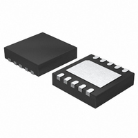
LTC2484CDD#PBF Linear Technology, LTC2484CDD#PBF Datasheet - Page 24

LTC2484CDD#PBF
Manufacturer Part Number
LTC2484CDD#PBF
Description
IC ADC 24BIT 10-DFN
Manufacturer
Linear Technology
Datasheet
1.LTC2484CDDTRPBF.pdf
(42 pages)
Specifications of LTC2484CDD#PBF
Number Of Bits
24
Sampling Rate (per Second)
6.8
Data Interface
MICROWIRE™, Serial, SPI™
Number Of Converters
1
Power Dissipation (max)
480µW
Voltage Supply Source
Single Supply
Operating Temperature
0°C ~ 70°C
Mounting Type
Surface Mount
Package / Case
10-WFDFN Exposed Pad
Number Of Elements
1
Resolution
24Bit
Architecture
Delta-Sigma
Sample Rate
0.0075KSPS
Input Polarity
Bipolar
Input Type
Voltage
Rated Input Volt
±2.75V
Differential Input
Yes
Power Supply Requirement
Single
Single Supply Voltage (typ)
3.3/5V
Single Supply Voltage (min)
2.7V
Single Supply Voltage (max)
5.5V
Dual Supply Voltage (typ)
Not RequiredV
Dual Supply Voltage (min)
Not RequiredV
Dual Supply Voltage (max)
Not RequiredV
Integral Nonlinearity Error
10ppm of Vref
Operating Temp Range
0C to 70C
Operating Temperature Classification
Commercial
Mounting
Surface Mount
Pin Count
10
Package Type
DFN EP
Input Signal Type
Differential
Lead Free Status / RoHS Status
Lead free / RoHS Compliant
Available stocks
Company
Part Number
Manufacturer
Quantity
Price
LTC2484
APPLICATIONS INFORMATION
Internal Serial Clock, 3-Wire I/O,
Continuous Conversion
This timing mode uses a 3-wire interface. The conversion
result is shifted out of the device by an internally gener-
ated serial clock (SCK) signal, see Figure 10. CS may be
permanently tied to ground, simplifying the user interface
or transmission over an isolation barrier.
The internal serial clock mode is selected at the end of the
power-on reset (POR) cycle. The POR cycle is concluded
approximately 1ms after V
pull-up is active during the POR cycle; therefore, the internal
serial clock timing mode is automatically selected if SCK
is not externally driven LOW (if SCK is loaded such that
the internal pull-up cannot pull the pin HIGH, the external
SCK mode will be selected).
During the conversion, the SCK and the serial data output
pin (SDO) are HIGH (EOC = 1). Once the conversion is
24
(INTERNAL)
SDO
SCK
SDI*
CS
CONVERSION
DON’T CARE
BIT 23
EOC
EN
CC
exceeds 2V. An internal weak
BIT 22
Figure 10. Internal Serial Clock, CS = 0 Continuous Operation
GS2
BIT 21
SIG
GS1
BIT 20
MSB
GS0
0.1V TO V
REFERENCE
VOLTAGE
ANALOG
BIT 19
INPUT
1μF
2.7V TO 5.5V
IM
CC
2
3
4
5
BIT 18
V
V
IN
IN
CC
REF
FA
+
–
LTC2484
complete, SCK and SDO go LOW (EOC = 0) indicating
the conversion has fi nished and the device has entered
the low power sleep state. The part remains in the sleep
state a minimum amount of time (1/2 the internal SCK
period) then immediately begins outputting data. The
data input/output cycle begins on the fi rst rising edge of
SCK and ends after the 32nd rising edge. The input data
is then shifted in via the SDI pin on the rising edge of
SCK (including the fi rst rising edge) and the output data
is shifted out of the SDO pin on each falling edge of SCK.
The internally generated serial clock is output to the SCK
pin. This signal may be used to shift the conversion result
into external circuitry. EOC can be latched on the fi rst ris-
ing edge of SCK and the last bit of the conversion result
can be latched on the 32nd rising edge of SCK. After the
32nd rising edge, SDO goes HIGH (EOC = 1) indicating a
new conversion is in progress. SCK remains HIGH during
the conversion.
DATA OUTPUT
BIT 17
SDO
GND
SCK
SDI
CS
f
O
FB
7
6
8
10
9
1
BIT 16
INT/EXT CLOCK
SPD
3-WIRE
SPI INTERFACE
V
CC
BIT 4
DON’T CARE
10k
LSB
BIT 0
IM
CONVERSION
2484fc
2484 F10


