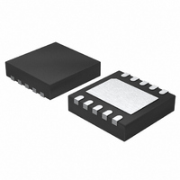
LTC2484CDD#PBF Linear Technology, LTC2484CDD#PBF Datasheet - Page 28

LTC2484CDD#PBF
Manufacturer Part Number
LTC2484CDD#PBF
Description
IC ADC 24BIT 10-DFN
Manufacturer
Linear Technology
Datasheet
1.LTC2484CDDTRPBF.pdf
(42 pages)
Specifications of LTC2484CDD#PBF
Number Of Bits
24
Sampling Rate (per Second)
6.8
Data Interface
MICROWIRE™, Serial, SPI™
Number Of Converters
1
Power Dissipation (max)
480µW
Voltage Supply Source
Single Supply
Operating Temperature
0°C ~ 70°C
Mounting Type
Surface Mount
Package / Case
10-WFDFN Exposed Pad
Number Of Elements
1
Resolution
24Bit
Architecture
Delta-Sigma
Sample Rate
0.0075KSPS
Input Polarity
Bipolar
Input Type
Voltage
Rated Input Volt
±2.75V
Differential Input
Yes
Power Supply Requirement
Single
Single Supply Voltage (typ)
3.3/5V
Single Supply Voltage (min)
2.7V
Single Supply Voltage (max)
5.5V
Dual Supply Voltage (typ)
Not RequiredV
Dual Supply Voltage (min)
Not RequiredV
Dual Supply Voltage (max)
Not RequiredV
Integral Nonlinearity Error
10ppm of Vref
Operating Temp Range
0C to 70C
Operating Temperature Classification
Commercial
Mounting
Surface Mount
Pin Count
10
Package Type
DFN EP
Input Signal Type
Differential
Lead Free Status / RoHS Status
Lead free / RoHS Compliant
Available stocks
Company
Part Number
Manufacturer
Quantity
Price
LTC2484
APPLICATIONS INFORMATION
Reference Current
In a similar fashion, the LTC2484 samples the differential
reference pins V
of charge to and from the external driving circuits thus
producing a dynamic reference current. This current does
not change the converter offset, but it may degrade the
gain and INL performance. The effect of this current can
be analyzed in two distinct situations.
For relatively small values of the external reference capaci-
tors (C
settles almost completely and relatively large values for
the source impedance result in only small errors. Such
values for C
gain performance without signifi cant benefi ts of reference
fi ltering and the user is advised to avoid them.
Larger values of reference capacitors (C
required as reference fi lters in certain confi gurations. Such
28
REF
Figure 13. +FS Error vs R
< 1nF), the voltage on the sampling capacitor
REF
–20
–40
–80
–60
80
60
40
20
0
1
V
V
V
V
f
T
REF
will deteriorate the converter offset and
O
CC
REF
IN
IN
A
= GND
= 25°C
+
–
= 5V
= 3.75V
= 1.25V
= 5V
+
10
and GND transferring small amount
C
100
R
IN
SOURCE
= 1nF, 0.1μF, 1μF
SOURCE
(Ω)
1k
C
IN
C
= 100pF
IN
V
V
INCM
INCM
= 0pF
at IN
10k
REF
+ 0.5V
– 0.5V
Figure 12. An RC Network at IN
+
2484 F13
> 1nF) may be
or IN
100k
IN
IN
–
R
R
SOURCE
SOURCE
C
C
IN
IN
capacitors will average the reference sampling charge and
the external source resistance will see a quasi constant
reference differential impedance.
In the following discussion, it is assumed the input and
reference common mode are the same. Using internal
oscillator for 60Hz mode, the typical differential reference
resistance is 1MΩ which generates a full-scale (V
error of 0.51ppm for each ohm of source resistance driving
the V
resistance is 1.1MΩ and the resulting full-scale error is
0.46ppm for each ohm of source resistance driving the
V
is 1.2MΩ and the resulting full-scale error is 0.42ppm for
each ohm of source resistance driving the V
f
(external conversion clock operation), the typical differen-
tial reference resistance is 0.30 • 10
ohm of source resistance driving the V
O
REF
is driven by an external oscillator with a frequency f
pin. For 50Hz mode, the related difference resistance
REF
C
C
PAR
20pF
PAR
20pF
+
Figure 14. –FS Error vs R
pin. For 50Hz/60Hz mode, the related difference
and IN
–20
–40
–80
–60
80
60
40
20
0
IN
IN
LTC2484
1
+
–
V
V
V
V
f
T
–
O
A
CC
REF
IN
IN
2484 F12
= GND
= 25°C
+
–
= 5V
= 1.25V
= 3.75V
= 5V
10
100
R
SOURCE
C
IN
= 1nF, 0.1μF, 1μF
(Ω)
SOURCE
C
1k
IN
= 100pF
C
12
IN
10k
at IN
= 0pF
/f
REF
EOSC
2484 F14
+
100k
REF
pin will result
or IN
Ω and each
REF
pin. When
–
/2) gain
EOSC
2484fc


