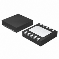
LTC2484CDD#PBF Linear Technology, LTC2484CDD#PBF Datasheet - Page 5

LTC2484CDD#PBF
Manufacturer Part Number
LTC2484CDD#PBF
Description
IC ADC 24BIT 10-DFN
Manufacturer
Linear Technology
Datasheet
1.LTC2484CDDTRPBF.pdf
(42 pages)
Specifications of LTC2484CDD#PBF
Number Of Bits
24
Sampling Rate (per Second)
6.8
Data Interface
MICROWIRE™, Serial, SPI™
Number Of Converters
1
Power Dissipation (max)
480µW
Voltage Supply Source
Single Supply
Operating Temperature
0°C ~ 70°C
Mounting Type
Surface Mount
Package / Case
10-WFDFN Exposed Pad
Number Of Elements
1
Resolution
24Bit
Architecture
Delta-Sigma
Sample Rate
0.0075KSPS
Input Polarity
Bipolar
Input Type
Voltage
Rated Input Volt
±2.75V
Differential Input
Yes
Power Supply Requirement
Single
Single Supply Voltage (typ)
3.3/5V
Single Supply Voltage (min)
2.7V
Single Supply Voltage (max)
5.5V
Dual Supply Voltage (typ)
Not RequiredV
Dual Supply Voltage (min)
Not RequiredV
Dual Supply Voltage (max)
Not RequiredV
Integral Nonlinearity Error
10ppm of Vref
Operating Temp Range
0C to 70C
Operating Temperature Classification
Commercial
Mounting
Surface Mount
Pin Count
10
Package Type
DFN EP
Input Signal Type
Differential
Lead Free Status / RoHS Status
Lead free / RoHS Compliant
Available stocks
Company
Part Number
Manufacturer
Quantity
Price
TIMING CHARACTERISTICS
SYMBOL
f
t
t
t
t
f
D
f
t
t
t
t
t
t
t
t4
t
t
t
t
t
t
range, otherwise specifi cations are at T
Note 1: Stresses beyond those listed under Absolute Maximum Ratings
may cause permanent damage to the device. Exposure to any Absolute
Maximum Rating condition for extended periods may affect device
reliability and lifetime
Note 2: All voltage values are with respect to GND.
Note 3: V
Note 4: Use internal conversion clock or external conversion clock source
with f
Note 5: Guaranteed by design, not subject to test.
Note 6: Integral nonlinearity is defi ned as the deviation of a code from a
straight line passing through the actual endpoints of the transfer curve.
The deviation is measured from the center of the quantization band.
Note 7: 50Hz mode (internal oscillator) or f
(external oscillator).
EOSC
HEO
LEO
ISCK
ESCK
LESCK
HESCK
DOUT_ISCK
DOUT_ESCK
1
KQMAX
KQMIN
5
7
8
CONV_1
CONV_2
2
3
6
ISCK
V
V
REFCM
IN
EOSC
= IN
CC
= 307.2kHz unless otherwise specifi ed.
= V
+
= 2.7V to 5.5V unless otherwise specifi ed.
– IN
REF
–
PARAMETER
External Oscillator Frequency Range
External Oscillator High Period
External Oscillator Low Period
Conversion Time for 1x Speed Mode
Conversion Time for 2x Speed Mode
Internal SCK Frequency
Internal SCK Duty Cycle
External SCK Frequency Range
External SCK Low Period
External SCK High Period
Internal SCK 32-Bit Data Output Time
External SCK 32-Bit Data Output Time
CS↓ to SDO Low
CS↑ to SDO Hi-Z
CS↓ to SCK↓
CS↓ to SCK↑
SCK↓ to SDO Valid
SDO Hold After SCK↓
SCK Set-Up Before CS↓
SCK Hold After CS↓
SDI Setup Before SCK↑
SDI Hold After SCK↑
/2, FS = 0.5V
, V
IN(CM)
= (IN
REF
+
+ IN
–
)/2
EOSC
A
= 256kHz ±2%
= 25°C. (Note 3)
The
CONDITIONS
(Note 15)
50Hz Mode
60Hz Mode
Simultaneous 50Hz/60Hz Mode
External Oscillator
50Hz Mode
60Hz Mode
Simultaneous 50Hz/60Hz Mode
External Oscillator
Internal Oscillator (Note 10)
External Oscillator (Notes 10, 11)
(Note 10)
(Note 10)
(Note 10)
(Note 10)
Internal Oscillator (Notes 10, 12)
External Oscillator (Notes 10, 11)
(Note 10)
(Note 10)
(Note 10)
(Note 5)
(Note 5)
(Note 5)
l
denotes the specifi cations which apply over the full operating temperature
Note 8: 60Hz mode (internal oscillator) or f
(external oscillator).
Note 9: Simultaneous 50Hz/60Hz mode (internal oscillator) or
f
Note 10: The SCK can be confi gured in external SCK mode or internal SCK
mode. In external SCK mode, the SCK pin is used as digital input and the
driving clock is f
output and the output clock signal during the data output is f
Note 11: The external oscillator is connected to the f
oscillator frequency, f
Note 12: The converter uses the internal oscillator.
Note 13: The output noise includes the contribution of the internal
calibration operations.
Note 14: Guaranteed by design and test correlation.
Note 15: Refer to Applications Information section for performance
vs data rate graphs.
Note 16: For V
EOSC
= 280kHz ±2% (external oscillator).
CC
ESCK
< 3V, V
l
l
l
l
l
l
l
l
l
l
l
l
l
l
l
l
l
l
l
l
l
l
l
l
l
l
l
l
. In internal SCK mode, the SCK pin is used as digital
EOSC
IH
, is expressed in kHz.
is 2.5V for pin f
0.125
0.125
157.2
131.0
144.1
MIN
78.7
65.6
72.2
0.81
125
125
100
100
10
45
50
50
15
0
0
0
20556/f
41036/f
256/f
32/f
ESCK
f
EOSC
EOSC
160.3
133.6
146.9
EOSC
EOSC
80.3
66.9
73.6
38.4
0.83
TYP
O
EOSC
.
(in kHz)
(in kHz)
/8
(in kHz)
(in kHz)
= 307.2kHz ±2%
LTC2484
O
pin. The external
163.5
136.3
149.9
MAX
4000
4000
81.9
68.2
75.1
0.85
200
200
200
200
100
100
55
50
ISCK
.
UNITS
2484fc
5
kHz
kHz
kHz
kHz
ms
ms
ms
ms
ms
ms
ms
ms
ms
ms
ms
μs
μs
ns
ns
ns
ns
ns
ns
ns
ns
ns
ns
ns
ns
%


