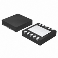
LTC2484CDD#PBF Linear Technology, LTC2484CDD#PBF Datasheet - Page 29

LTC2484CDD#PBF
Manufacturer Part Number
LTC2484CDD#PBF
Description
IC ADC 24BIT 10-DFN
Manufacturer
Linear Technology
Datasheet
1.LTC2484CDDTRPBF.pdf
(42 pages)
Specifications of LTC2484CDD#PBF
Number Of Bits
24
Sampling Rate (per Second)
6.8
Data Interface
MICROWIRE™, Serial, SPI™
Number Of Converters
1
Power Dissipation (max)
480µW
Voltage Supply Source
Single Supply
Operating Temperature
0°C ~ 70°C
Mounting Type
Surface Mount
Package / Case
10-WFDFN Exposed Pad
Number Of Elements
1
Resolution
24Bit
Architecture
Delta-Sigma
Sample Rate
0.0075KSPS
Input Polarity
Bipolar
Input Type
Voltage
Rated Input Volt
±2.75V
Differential Input
Yes
Power Supply Requirement
Single
Single Supply Voltage (typ)
3.3/5V
Single Supply Voltage (min)
2.7V
Single Supply Voltage (max)
5.5V
Dual Supply Voltage (typ)
Not RequiredV
Dual Supply Voltage (min)
Not RequiredV
Dual Supply Voltage (max)
Not RequiredV
Integral Nonlinearity Error
10ppm of Vref
Operating Temp Range
0C to 70C
Operating Temperature Classification
Commercial
Mounting
Surface Mount
Pin Count
10
Package Type
DFN EP
Input Signal Type
Differential
Lead Free Status / RoHS Status
Lead free / RoHS Compliant
Available stocks
Company
Part Number
Manufacturer
Quantity
Price
APPLICATIONS INFORMATION
in 1.67 • 10
–FS errors for various combinations of source resistance
seen by the V
to that pin are shown in Figures 15-18.
In addition to this gain error, the converter INL per-
formance is degraded by the reference source imped-
ance. The INL is caused by the input dependent terms
–V
pin current as expressed in Figure 11. When using internal
IN
2
Figure 15. +FS Error vs R
Figure 17. +FS Error vs R
/(V
REF
100
–10
500
400
300
200
–6
90
80
70
60
50
40
30
20
10
• R
0
0
REF
0
0
• f
V
V
V
V
f
T
V
V
V
V
f
T
EQ
O
O
A
CC
REF
IN
IN
A
CC
REF
IN
IN
EOSC
= GND
= GND
= 25°C
= 25°C
+
–
pin and external capacitance connected
+
–
) – (0.5 • V
= 5V
= 5V
= 3.75V
= 1.25V
= 3.75V
= 1.25V
= 5V
= 5V
C
200
10
C
REF
C
REF
REF
ppm gain error. The typical +FS and
C
= 0.001μF
REF
= 0.01μF
= 100pF
= 0pF
100
400
R
R
SOURCE
SOURCE
SOURCE
SOURCE
REF
C
REF
600
(Ω)
(Ω)
• D
1k
= 1μF, 10μF
at V
at V
T
C
)/R
REF
C
REF
800
10k
REF
REF
= 0.01μF
EQ
= 0.1μF
2484 F15
(Small C
2484 F17
(Large C
in the reference
100k
1000
REF
REF
)
)
oscillator and 60Hz mode, every 100Ω of reference source
resistance translates into about 0.67ppm additional INL
error. When using internal oscillator and 50Hz/60Hz mode,
every 100Ω of reference source resistance translates into
about 0.61ppm additional INL error. When using internal
oscillator and 50Hz mode, every 100Ω of reference source
resistance translates into about 0.56ppm additional INL
error. When f
frequency f
Figure 18. –FS Error vs R
Figure 16. –FS Error vs R
–100
–300
–400
–500
–200
EOSC
–10
–20
–30
–40
–50
–60
–70
–80
–90
10
0
0
O
0
0
V
V
V
V
f
T
V
V
V
V
f
T
O
O
is driven by an external oscillator with a
A
, every 100Ω of source resistance driving
A
CC
REF
IN
IN
CC
REF
IN
IN
= GND
= GND
= 25°C
= 25°C
+
–
+
–
C
C
= 5V
= 5V
REF
= 1.25V
= 3.75V
= 1.25V
= 3.75V
= 5V
C
= 5V
REF
C
200
REF
10
REF
C
= 1μF, 10μF
= 0.001μF
REF
= 0.01μF
= 100pF
= 0pF
400
R
100
R
SOURCE
SOURCE
SOURCE
SOURCE
600
(Ω)
(Ω)
1k
at V
C
at V
REF
C
REF
800
10k
= 0.01μF
REF
REF
= 0.1μF
LTC2484
2484 F18
(Large C
2484 F16
(Small C
1000
100k
REF
REF
29
)
)
2484fc


