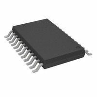
AD7739BRU Analog Devices Inc, AD7739BRU Datasheet - Page 13

AD7739BRU
Manufacturer Part Number
AD7739BRU
Description
IC ADC 24BIT 8-CH 24-TSSOP
Manufacturer
Analog Devices Inc
Datasheet
1.AD7739BRUZ.pdf
(32 pages)
Specifications of AD7739BRU
Rohs Status
RoHS non-compliant
Number Of Bits
24
Sampling Rate (per Second)
15.1k
Data Interface
DSP, MICROWIRE™, QSPI™, Serial, SPI™
Number Of Converters
1
Power Dissipation (max)
100mW
Voltage Supply Source
Analog and Digital
Operating Temperature
-40°C ~ 105°C
Mounting Type
Surface Mount
Package / Case
24-TSSOP (0.173", 4.40mm Width)
For Use With
EVAL-AD7739EBZ - BOARD EVAL FOR AD7739
Available stocks
Company
Part Number
Manufacturer
Quantity
Price
Company:
Part Number:
AD7739BRUZ
Manufacturer:
ADI
Quantity:
1 000
Company:
Part Number:
AD7739BRUZ
Manufacturer:
Analog Devices Inc
Quantity:
1 859
Part Number:
AD7739BRUZ
Manufacturer:
ADI/亚德诺
Quantity:
20 000
Company:
Part Number:
AD7739BRUZ-REEL7
Manufacturer:
ADI
Quantity:
1 000
Pin No.
8
9–16
17
18
19
20
21
22
23
24
Mnemonic
SYNC/P1
AIN0–AIN7
REFIN(+)
REFIN(–)
AGND
RDY
DOUT
DIN
DV
DGND
DD
Description
Analog Inputs.
Positive Terminal of the Differential Reference Input. REFIN(+) voltage potential can lie
anywhere between AV
connected to a 2.5 V reference voltage.
Negative Terminal of the Differential Reference Input. REFIN(–) voltage potential can lie
anywhere between AV
connected to a 0 V reference voltage.
Ground Reference Point for Analog Circuitry.
Logic Output. Used as a status output in both conversion mode and calibration mode. In
conversion mode, a falling edge on this output indicates that either any channel or all
channels have unread data available, according to the RDYFN bit in the I/O port register.
In calibration mode, a falling edge on this output indicates that calibration is complete
(see the Digital Interface Description section for details).
Serial Data Output. Serial data is read from the output shift register on the part. This
output shift register can contain information from any AD7739 register, depending on
the address bits of the communications register.
Serial Data Input (Schmitt Triggered). Serial data is written to the input shift register on
the part. Data from this input shift register is transferred to any AD7739 register,
depending on the address bits of the communications register.
Digital Supply Voltage, 3 V or 5 V Nominal.
Ground Reference Point for Digital Circuitry.
SYNC/Digital Input/Digital Output. The pin direction is determined by the P1 DIR bit;
the digital value can be read/written as the P1 bit in the I/O port register. When the SYNC
bit in the I/O port register is set to 1, then the SYNC/P1 pin can be used to synchronize
the AD7739 modulator and digital filter with other devices in the system. The digital
voltage is referenced to the analog supplies. When configured as an input, the pin should
be tied high or low.
Rev. 0 | Page 13 of 32
DD
DD
and AGND. In normal circuit configuration, this pin should be
and AGND. In normal circuit configuration, this pin should be
AD7739


