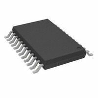
AD7739BRU Analog Devices Inc, AD7739BRU Datasheet - Page 5

AD7739BRU
Manufacturer Part Number
AD7739BRU
Description
IC ADC 24BIT 8-CH 24-TSSOP
Manufacturer
Analog Devices Inc
Datasheet
1.AD7739BRUZ.pdf
(32 pages)
Specifications of AD7739BRU
Rohs Status
RoHS non-compliant
Number Of Bits
24
Sampling Rate (per Second)
15.1k
Data Interface
DSP, MICROWIRE™, QSPI™, Serial, SPI™
Number Of Converters
1
Power Dissipation (max)
100mW
Voltage Supply Source
Analog and Digital
Operating Temperature
-40°C ~ 105°C
Mounting Type
Surface Mount
Package / Case
24-TSSOP (0.173", 4.40mm Width)
For Use With
EVAL-AD7739EBZ - BOARD EVAL FOR AD7739
Available stocks
Company
Part Number
Manufacturer
Quantity
Price
Company:
Part Number:
AD7739BRUZ
Manufacturer:
ADI
Quantity:
1 000
Company:
Part Number:
AD7739BRUZ
Manufacturer:
Analog Devices Inc
Quantity:
1 859
Part Number:
AD7739BRUZ
Manufacturer:
ADI/亚德诺
Quantity:
20 000
Company:
Part Number:
AD7739BRUZ-REEL7
Manufacturer:
ADI
Quantity:
1 000
Parameter
POWER REQUIREMENTS
1
2
3
4
5
6
7
8
9
10
11
12
13
14
See Typical Performance Characteristics.
Specifications before calibration. Channel system calibration reduces these errors to the order of the noise.
Specifications before calibration. ADC zero-scale self-calibration or channel zero-scale system calibration reduce this error to the order of the noise.
For specified performance. The output data span corresponds to the specified nominal input voltage range. The ADC is functional outside the nominal input voltage
For specified performance. If the analog input absolute voltage (referred to AGND) changes more than 0.5 V during one conversion time, the result could be affected
Specification is not production tested, but is supported by characterization data at initial product release.
Applies after the zero-scale and full-scale calibration. The negative full-scale error represents the remaining error after removing the offset and gain error.
range, but the performance might degrade. Outside the nominal input voltage range, the OVR bit in the channel status register is set and the channel data register
value depends on the CLAMP bit in the mode register. See the register and circuit descriptions for details.
by distortion in the input buffer. This limit does not apply to analog input absolute voltages below 3 V.
If chopping is enabled or when switching between channels, a dynamic current charges the capacitance of the multiplexer. See the circuit description for details.
For specified performance. Part is functional with lower V
Dynamic current charging the sigma-delta modulator input switching capacitor.
Outside the specified calibration range, calibration is possible but the performance may degrade.
These logic output levels apply to the MCLK OUT output when it is loaded with a single CMOS load.
With external MCLK, MCLKOUT disabled (CLKDIS bit set in the mode register).
External MCLKIN = 0 V or DV
AV
DV
AV
AV
AV
DV
DV
Power Dissipation (Normal Mode)
Power Dissipation
(Reduced Power Mode)
Power Dissipation
(Reduced Power Mode)
AV
(Standby Mode)
Power Dissipation (Standby Mode)
DD
DD
DD
DD
DD
DD
DD
DD
to AGND Voltage
Current (Normal Mode)
Current (Reduced Power Mode)
Current (Internal Buffer Off)
+ DV
to DGND Voltage
Current (Normal Mode)
Current (Normal Mode)
DD
Current
14
DD
13
13
, digital inputs = 0 V or DV
13
13
13
14
Min
4.75
4.75
2.70
DD
REF
, P0 and P1 = 0 V or AV
.
Typ
13.6
9.2
8.5
2.7
1.0
85
60
50
80
500
Rev. 0 | Page 5 of 32
DD
.
Max
5.25
5.25
3.60
16
11
3
1.5
100
70
Unit
V
V
V
mA
mA
mA
mA
mA
mW
mW
mW
µA
µW
Test Conditions/Comments
MCLK = 4 MHz
DV
DV
DV
DV
DD
DD
DD
DD
= 5 V
= 3 V
= 5 V, MCLK = 4 MHz
= 3 V, MCLK = 4 MHz
AD7739


