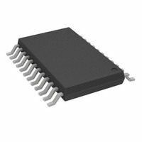
AD7739BRU Analog Devices Inc, AD7739BRU Datasheet - Page 20

AD7739BRU
Manufacturer Part Number
AD7739BRU
Description
IC ADC 24BIT 8-CH 24-TSSOP
Manufacturer
Analog Devices Inc
Datasheet
1.AD7739BRUZ.pdf
(32 pages)
Specifications of AD7739BRU
Rohs Status
RoHS non-compliant
Number Of Bits
24
Sampling Rate (per Second)
15.1k
Data Interface
DSP, MICROWIRE™, QSPI™, Serial, SPI™
Number Of Converters
1
Power Dissipation (max)
100mW
Voltage Supply Source
Analog and Digital
Operating Temperature
-40°C ~ 105°C
Mounting Type
Surface Mount
Package / Case
24-TSSOP (0.173", 4.40mm Width)
For Use With
EVAL-AD7739EBZ - BOARD EVAL FOR AD7739
Available stocks
Company
Part Number
Manufacturer
Quantity
Price
Company:
Part Number:
AD7739BRUZ
Manufacturer:
ADI
Quantity:
1 000
Company:
Part Number:
AD7739BRUZ
Manufacturer:
Analog Devices Inc
Quantity:
1 859
Part Number:
AD7739BRUZ
Manufacturer:
ADI/亚德诺
Quantity:
20 000
Company:
Part Number:
AD7739BRUZ-REEL7
Manufacturer:
ADI
Quantity:
1 000
AD7739
CHANNEL CONVERSION TIME REGISTERS
8 Bits, Read/Write Registers, Address 0x30–0x37h, Default Value 0x91
The conversion time registers enable or disable chopping and configure the digital filter for a particular channel. This register value affects
the conversion time, frequency response, and noise performance of the ADC.
Bit
Mnemonic
Default
Bit
7
6–0
MODE REGISTER
8 Bits, Read/Write Register, Address 0x38–0x3F, Default Value 0x00
The mode register configures the part and determines its operating mode. Writing to the mode register clears the ADC status register, sets
the RDY pin to a logic high level, exits all current operations, and starts the mode specified by the mode bits.
The AD7739 contains only one mode register. The two LSBs of the address are used for writing to the mode register to specify the channel
selected for the operation determined by the MD2 to MD0 bits. Only the address 0x38 must be used for reading from the mode register.
Bit
Mnemonic
Default
Bit
7–5
Mnemonic
CHOP
FW
Mnemonic
MD2–MD0
Bit 7
CHOP
1
Description
Chopping Enable Bit. Set to 1 to apply chopping mode for a particular channel.
CHOP = 1, single conversion or continuous conversion with one channel enabled.
Conversion Time (µs) = (FW × 128 + 262)/MCLK Frequency (MHz), the FW range is 2 to 127.
CHOP = 1, continuous conversion with two or more channels enabled.
Conversion Time (µs) = (FW × 128 + 263)/MCLK Frequency (MHz), the FW range is 2 to 127.
CHOP = 0, single conversion or continuous conversion with one channel enabled.
Conversion Time (µs) = (FW × 64 + 213)/MCLK Frequency (MHz), the FW range is 3 to 127.
CHOP = 0, continuous conversion with two or more channels enabled.
Conversion Time (µs) = (FW × 64 + 214)/MCLK Frequency (MHz), the FW range is 3 to 127.
Bit 7
MD2
0
Description
Mode Bits. These three bits determine the AD7739 operation mode. Writing a new value to the mode bits will
exit the part from the mode in which it has been operating and place it in the newly requested mode
immediately. The function of the mode bits is described in more detail below.
MD2
0
0
0
0
1
1
1
1
MD1
0
0
1
1
0
0
1
1
Bit 6
Bit 6
MD1
0
MD0
0
1
0
1
0
1
0
1
Channel Zero-Scale System Calibration
Channel Full-Scale System Calibration
Mode
Idle
Continuous Conversion
Single Conversion
Power-Down (Standby)
ADC Zero-Scale Self-Calibration
ADC Full-Scale Self-Calibration (for 2.5 V)
Bit 5
Bit 5
MD0
0
Rev. 0 | Page 20 of 32
Bit 4
Bit 4
CLKDIS
0
FW (7-Bit Filter Word)
Bit 3
Bit 3
DUMP
0
0x11
Address Used for Mode Register
Write Specifies:
First Channel to Start Converting
Channel to Convert
Conversion Time for Calibration
Conversion Time for Calibration
Channel to Calibrate
Channel to Calibrate
Bit 2
Bit 2
0
Cont RD
Bit 1
Bit 1
24/16 BIT
0
Bit 0
Bit 0
CLAMP
0


