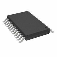
AD7739BRU Analog Devices Inc, AD7739BRU Datasheet - Page 6

AD7739BRU
Manufacturer Part Number
AD7739BRU
Description
IC ADC 24BIT 8-CH 24-TSSOP
Manufacturer
Analog Devices Inc
Datasheet
1.AD7739BRUZ.pdf
(32 pages)
Specifications of AD7739BRU
Rohs Status
RoHS non-compliant
Number Of Bits
24
Sampling Rate (per Second)
15.1k
Data Interface
DSP, MICROWIRE™, QSPI™, Serial, SPI™
Number Of Converters
1
Power Dissipation (max)
100mW
Voltage Supply Source
Analog and Digital
Operating Temperature
-40°C ~ 105°C
Mounting Type
Surface Mount
Package / Case
24-TSSOP (0.173", 4.40mm Width)
For Use With
EVAL-AD7739EBZ - BOARD EVAL FOR AD7739
Available stocks
Company
Part Number
Manufacturer
Quantity
Price
Company:
Part Number:
AD7739BRUZ
Manufacturer:
ADI
Quantity:
1 000
Company:
Part Number:
AD7739BRUZ
Manufacturer:
Analog Devices Inc
Quantity:
1 859
Part Number:
AD7739BRUZ
Manufacturer:
ADI/亚德诺
Quantity:
20 000
Company:
Part Number:
AD7739BRUZ-REEL7
Manufacturer:
ADI
Quantity:
1 000
AD7739
TIMING SPECIFICATIONS
Table 2. (AV
unless otherwise noted.)
Parameter
Master Clock Range
Read Operation
Write Operation
1
2
3
4
These numbers are measured with the load circuit of Figure 4 and defined as the time required for the output to cross the V
Sample tested during initial release to ensure compliance. All input signals are specified with tr = tf = 5 ns (10% to 90% of DV
1.6 V. See Figure 2 and Figure 3.
This specification is relevant only if CS goes low while SCLK is low.
These numbers are derived from the measured time taken by the data output to change 0.5 V when loaded with the circuit of Figure 4. The measured number is then
extrapolated back to remove effects of charging or discharging the 50 pF capacitor. This means that the times quoted in the Timing Specifications are the true bus
relinquish times of the part and as such are independent of external bus loading capacitances.
t
t
t
t
t
t
t
t
t
t
t
t
t
t
t
1
2
4
5
5A
6
7
8
9
11
12
13
14
15
16
2
4
2, 3
DD
= 5 V ± 5%; DV
1
Min
1
1
50
500
0
0
0
0
0
50
50
0
10
0
30
25
50
50
0
DD
= 2.7 V to 3.6 V, or 5 V ± 5%; Input Logic 0 = 0 V; Logic 1 = DV
Typ
Max
6.144
4
60
80
60
80
80
Unit
MHz
MHz
ns
ns
ns
ns
ns
ns
ns
ns
ns
ns
ns
ns
ns
ns
ns
ns
ns
Rev. 0 | Page 6 of 32
Test Conditions/Comments
Reduced Power Mode
SYNC Pulsewidth
RESET Pulsewidth
CS Falling Edge to SCLK Falling Edge Setup Time
SCLK Falling Edge to Data Valid Delay
DV
DV
CS Falling Edge to Data Valid Delay
DV
DV
SCLK High Pulsewidth
SCLK Low Pulsewidth
CS Rising Edge after SCLK Rising Edge Hold Time
Bus Relinquish Time after SCLK Rising Edge
CS Falling Edge to SCLK Falling Edge Setup
Data Valid to SCLK Rising Edge Setup Time
Data Valid after SCLK Rising Edge Hold Time
SCLK High Pulsewidth
SCLK Low Pulsewidth
CS Rising Edge after SCLK Rising Edge Hold Time
DD
DD
DD
DD
of 4.75 V to 5.25 V
of 2.7 V to 3.3 V
of 4.75 V to 5.25 V
of 2.7 V to 3.3 V
DD
OL
;
DD
or V
) and timed from a voltage level of
OH
limits.


