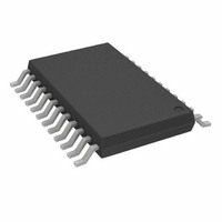
AD7739BRU Analog Devices Inc, AD7739BRU Datasheet - Page 29

AD7739BRU
Manufacturer Part Number
AD7739BRU
Description
IC ADC 24BIT 8-CH 24-TSSOP
Manufacturer
Analog Devices Inc
Datasheet
1.AD7739BRUZ.pdf
(32 pages)
Specifications of AD7739BRU
Rohs Status
RoHS non-compliant
Number Of Bits
24
Sampling Rate (per Second)
15.1k
Data Interface
DSP, MICROWIRE™, QSPI™, Serial, SPI™
Number Of Converters
1
Power Dissipation (max)
100mW
Voltage Supply Source
Analog and Digital
Operating Temperature
-40°C ~ 105°C
Mounting Type
Surface Mount
Package / Case
24-TSSOP (0.173", 4.40mm Width)
For Use With
EVAL-AD7739EBZ - BOARD EVAL FOR AD7739
Available stocks
Company
Part Number
Manufacturer
Quantity
Price
Company:
Part Number:
AD7739BRUZ
Manufacturer:
ADI
Quantity:
1 000
Company:
Part Number:
AD7739BRUZ
Manufacturer:
Analog Devices Inc
Quantity:
1 859
Part Number:
AD7739BRUZ
Manufacturer:
ADI/亚德诺
Quantity:
20 000
Company:
Part Number:
AD7739BRUZ-REEL7
Manufacturer:
ADI
Quantity:
1 000
ANALOG INPUT’S EXTENDED VOLTAGE RANGE
The AD7739 output data code span corresponds to the nominal
input voltage range. The ADC is functional outside the nominal
input voltage range, but the performance might degrade. The
sigma-delta modulator was designed to fully cover 16% analog
input overrange; outside this range, the performance might
degrade more rapidly.
When the CLAMP bit in the mode register is set to 1, the
channel data register will be digitally clamped to either all 0s or
all 1s when the analog input voltage goes outside the nominal
input voltage range.
As shown in Table 14 and Table 15, when CLAMP = 0, the data
reflects the analog input voltage outside the nominal voltage
range. In this case, the SIGN and OVR bits in the channel status
register should be considered along with the data register value
to decode the actual conversion result.
Note that the OVR bit in the channel status register is generated
digitally from the conversion result and indicates the sigma-
delta modulator (nominal) overrange. The OVR bit DOES NOT
indicate exceeding the AIN pin’s absolute voltage limits.
Table 14. Extended Input Voltage Range,
Nominal Voltage Range ±1.25 V, 16 Bits, CLAMP = 0
Input (V)
+1.45000
+1.25008
+1.25004
+1.25000
+0.00004
0.00000
–0.00004
–1.25000
–1.25004
–1.25008
–1.45000
Table 15. Extended Input Voltage Range,
Nominal Voltage Range +1.25 V, 16 Bits, CLAMP = 0
Input (V)
+1.45000
+1.25004
+1.25002
+1.25000
+0.00002
+0.00000
–0.00002
Data (hex)
0x28F5
0x0001
0x0000
0xFFFF
0x0001
0x0000
0x0000
Data (hex)
0x147B
0x0001
0x0000
0xFFFF
0x8001
0x8000
0x7FFF
0x0000
0xFFFF
0xFFFE
0xEB85
SIGN
0
0
0
0
0
0
1
SIGN
0
0
0
0
0
0
1
1
1
1
1
OVR
1
0
0
0
0
1
1
1
1
1
0
OVR
1
1
1
0
0
0
1
Rev. 0 | Page 29 of 32
VOLTAGE REFERENCE INPUTS
The AD7739 has a differential reference input, REF IN(+) and
REF IN(–). The common-mode range for these inputs is from
AGND to AV
specified operation is 2.5 V. Both reference inputs feature
dynamic load. Therefore, the reference inputs should be
connected to a low impedance reference voltage source.
External resistance/capacitance combinations may result in gain
errors on the part.
The output noise performance outlined in Table 4 through
Table 9 is for an analog input of 0 V and is unaffected by noise
on the reference. Obtaining the same noise performance as
shown in the noise tables over the full input range requires a
low noise reference source for the AD7739. If the reference
noise in the bandwidth of interest is excessive, it will degrade
the performance of the AD7739.
Recommended reference voltage sources for the AD7739
include the ADR421, AD780, REF43, and REF192.
REFERENCE DETECT
The AD7739 includes on-chip circuitry to detect if the part has
a valid reference for conversions. If the voltage between the
REFIN(+) and REFIN(–) pins goes below the NOREF trigger
voltage (0.5 V typ.) and the AD7739 is performing a conversion,
the NOREF bit in the channel status register is set.
I/O PORT
The AD7739 P0 pin can be used as a general-purpose digital
output or as a common analog input.
The P1 pin ( SYNC /P1) can be used as a general-purpose digital
I/O pin or to synchronize the AD7739 with other devices in the
system. When the SYNC bit in the I/O port register is set and
the SYNC pin is low, the AD7739 does not process any
conversion. If it is put into single conversion mode, continuous
conversion mode, or any calibration mode, the AD7739 waits
until the SYNC pin goes high and then starts operation. This
allows conversion to start from a known point in time, i.e., the
rising edge of the SYNC pin. When configured as input, the
SYNC pin should be tied high or low.
The digital P0 and P1 voltage is referenced to the analog
supplies.
DD
. The nominal differential reference voltage for
AD7739


