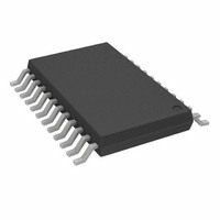
AD7739BRU Analog Devices Inc, AD7739BRU Datasheet - Page 17

AD7739BRU
Manufacturer Part Number
AD7739BRU
Description
IC ADC 24BIT 8-CH 24-TSSOP
Manufacturer
Analog Devices Inc
Datasheet
1.AD7739BRUZ.pdf
(32 pages)
Specifications of AD7739BRU
Rohs Status
RoHS non-compliant
Number Of Bits
24
Sampling Rate (per Second)
15.1k
Data Interface
DSP, MICROWIRE™, QSPI™, Serial, SPI™
Number Of Converters
1
Power Dissipation (max)
100mW
Voltage Supply Source
Analog and Digital
Operating Temperature
-40°C ~ 105°C
Mounting Type
Surface Mount
Package / Case
24-TSSOP (0.173", 4.40mm Width)
For Use With
EVAL-AD7739EBZ - BOARD EVAL FOR AD7739
Available stocks
Company
Part Number
Manufacturer
Quantity
Price
Company:
Part Number:
AD7739BRUZ
Manufacturer:
ADI
Quantity:
1 000
Company:
Part Number:
AD7739BRUZ
Manufacturer:
Analog Devices Inc
Quantity:
1 859
Part Number:
AD7739BRUZ
Manufacturer:
ADI/亚德诺
Quantity:
20 000
Company:
Part Number:
AD7739BRUZ-REEL7
Manufacturer:
ADI
Quantity:
1 000
ADC STATUS REGISTER
8 Bits, Read-Only Register, Address 0x04, Default Value 0x00
In conversion modes, the register bits reflect the individual channel status. When a conversion is complete, the corresponding channel
data register is updated and the corresponding RDY bit is set to 1. When the channel data register is read, the corresponding bit is reset
to 0. The bit is reset to 0 also when no read operation has taken place and the result of the next conversion is being updated to the channel
data register. Writing to the mode register resets all the bits to 0.
In calibration modes, all the register bits are reset to 0 while a calibration is in progress; all the register bits are set to 1 when the
calibration is complete.
The RDY pin output is related to the content of the ADC status register as defined by the RDYFN bit in the I/O port register. The RDY0
bit corresponds to Channel 0, the RDY1 bit corresponds to Channel 1, and so on.
Bit
Mnemonic
Default
CHECKSUM REGISTER
16 Bits, Read/Write Register, Address 0x05
This register is described in the Using the AD7732/AD7734/
AD7738/AD7739 Checksum Register application note
(www.analog.com/UploadedFiles/Application_Notes/71751876
AN626_0.pdf).
ADC ZERO-SCALE CALIBRATION REGISTER
24 Bits, Read/Write Register, Address 0x06,
Default Value 0x80 0000
This register holds the ADC zero-scale calibration coefficient.
The value in this register is used in conjunction with the value
in the ADC full-scale calibration register and the corresponding
channel zero-scale and channel full-scale calibration registers to
scale digitally the conversion results of all channels. The value
in this register is updated automatically following the execution
of an ADC zero-scale self-calibration. Writing this register is
possible in the idle mode only (see the Calibration section
for details).
ADC FULL-SCALE CALIBRATION REGISTER
24 Bits, Read/Write Register, Address 0x07,
Default Value 0x80 0000
This register holds the ADC full-scale calibration coefficient.
The value in this register is used in conjunction with the value
in the ADC zero-scale and the corresponding channel
zero-scale and channel full-scale calibration registers to scale
digitally the conversion results of all channels. The value in this
register is updated automatically following the execution of an
ADC full-scale self-calibration. Writing this register is possible
in the idle mode only. The ADC full-scale self-calibration
should be used only on +2.5 V and ±2.5 V input voltage ranges
(see the Calibration section for details).
Bit 7
RDY7
0
Bit 6
RDY6
0
Bit 5
RDY5
0
Rev. 0 | Page 17 of 32
Bit 4
RDY4
0
CHANNEL DATA REGISTERS
16 Bit/24 Bit, Read-Only Registers, Address 0x08–0x0F,
Default Width 16 Bits, Default Value 0x8000
These registers contain the most up-to-date conversion results
corresponding to each analog input channel. The 16-bit or
24-bit data width can be configured by setting the 24/16 bit in
the mode register. The relevant RDY bit in the channel status
register goes high when the result is updated. The RDY bit will
return low once the data register reading has begun. The RDY
pin can be configured to indicate when any channel has unread
data or waits until all enabled channels have unread data. If any
channel data register read operation is in progress when a new
result is updated, no update of the data register will occur. This
avoids having corrupted data. Reading the status registers can
be associated with reading the data registers in the dump mode.
Reading the status registers is always associated with reading
the data registers in the continuous read mode (see the Digital
Interface Description section for details).
Bit 3
RDY3
0
Bit 2
RDY2
0
Bit 1
RDY1
0
AD7739
Bit 0
RDY0
0


