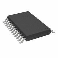
AD7739BRU Analog Devices Inc, AD7739BRU Datasheet - Page 24

AD7739BRU
Manufacturer Part Number
AD7739BRU
Description
IC ADC 24BIT 8-CH 24-TSSOP
Manufacturer
Analog Devices Inc
Datasheet
1.AD7739BRUZ.pdf
(32 pages)
Specifications of AD7739BRU
Rohs Status
RoHS non-compliant
Number Of Bits
24
Sampling Rate (per Second)
15.1k
Data Interface
DSP, MICROWIRE™, QSPI™, Serial, SPI™
Number Of Converters
1
Power Dissipation (max)
100mW
Voltage Supply Source
Analog and Digital
Operating Temperature
-40°C ~ 105°C
Mounting Type
Surface Mount
Package / Case
24-TSSOP (0.173", 4.40mm Width)
For Use With
EVAL-AD7739EBZ - BOARD EVAL FOR AD7739
Available stocks
Company
Part Number
Manufacturer
Quantity
Price
Company:
Part Number:
AD7739BRUZ
Manufacturer:
ADI
Quantity:
1 000
Company:
Part Number:
AD7739BRUZ
Manufacturer:
Analog Devices Inc
Quantity:
1 859
Part Number:
AD7739BRUZ
Manufacturer:
ADI/亚德诺
Quantity:
20 000
Company:
Part Number:
AD7739BRUZ-REEL7
Manufacturer:
ADI
Quantity:
1 000
AD7739
CONTINUOUS CONVERSION MODE
When the mode register is being written, the ADC status byte is
cleared and the RDY pin goes high, regardless of its previous
state. When the continuous conversion command is written to
the mode register, the ADC starts conversion on the channel
selected by the address of the mode register.
After the conversion is complete, the relevant channel data
register and channel status register are updated, the relevant
RDY bit in the ADC status register is set, and the AD7739
continues converting on the next enabled channel. The part will
cycle through all enabled channels until put into another mode
or reset. The cycle period will be the sum of all enabled
channels’ conversion times, set by the corresponding channel
conversion time registers.
The RDY bit is reset when the relevant channel data register is
being read. The behavior of the RDY pin depends on the
RDYFN bit in the I/O port register. When the RDYFN bit is 0,
the RDY pin goes low when any channel has unread data. When
the RDYFN bit is set to 1, the RDY pin will go low only if all
enabled channels have unread data.
INTERFACE
INTERFACE
INTERFACE
SERIAL
SERIAL
SERIAL
RDY
RDY
RDY
CONTINUOUS
CONVERSION
CONTINUOUS
CONVERSION
CONTINUOUS
CONVERSION
START
START
START
CH0 CONVERSION
CH0 CONVERSION
CH0 CONVERSION
Figure 21. Continuous Conversion, CH0 and CH1, No Data Read
Figure 19. Continuous Conversion, CH0 and CH1, RDYFN = 0
Figure 20. Continuous Conversion, CH0 and CH1, RDYFN = 1
CH1 CONVERSION
READ
DATA
CH1 CONVERSION
CH1 CONVERSION
CH0
Rev. 0 | Page 24 of 32
CH0 CONVERSION
CH0 CONVERSION
READ
DATA
CH0 CONVERSION
READ
DATA
CH1
CH0
If an ADC conversion result has not been read before a new
ADC conversion is completed, the new result will overwrite the
previous one. The relevant RDY bit goes low and the RDY pin
goes high for at least 163 MCLK cycles (~26.5 µs), indicating
when the data register is updated, and the previous conversion
data is lost.
If the data register is being read as an ADC conversion
completes, the data register will not be updated with the new
result (to avoid data corruption) and the new conversion
data is lost.
Figure 19 shows the digital interface signal’s sequence for the
continuous conversion mode with Channels 0 and 1 enabled
and the RDYFN bit set to 0. The RDY pin goes low and the data
register is read after each conversion. Figure 20 shows a similar
sequence but with the RDYFN bit set to 1. The RDY pin goes
low and all data registers are read after all conversions are
completed. Figure 21 shows the RDY pin when no data is read
from the AD7739.
READ
DATA
CH1
CH1 CONVERSION
READ
DATA
CH1 CONVERSION
CH1 CONVERSION
CH0
CH0 CONVERSION
CH0 CONVERSION
CH0 CONVERSION
READ
DATA
READ
DATA
CH1
CH0
READ
DATA
CH1
03742-0-020
03742-0-019
03742-0-021


