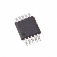
ISL95311UIU10Z-TK Intersil, ISL95311UIU10Z-TK Datasheet - Page 5

ISL95311UIU10Z-TK
Manufacturer Part Number
ISL95311UIU10Z-TK
Description
IC XDCP 128-TAP 50KOHM 10-MSOP
Manufacturer
Intersil
Series
XDCP™r
Datasheet
1.ISL95311WIU10Z-TK.pdf
(11 pages)
Specifications of ISL95311UIU10Z-TK
Taps
128
Resistance (ohms)
50K
Number Of Circuits
1
Temperature Coefficient
45 ppm/°C Typical
Memory Type
Non-Volatile
Interface
I²C, 2-Wire Serial
Voltage - Supply
2.7 V ~ 5.5 V
Operating Temperature
-40°C ~ 85°C
Mounting Type
Surface Mount
Package / Case
10-MSOP, Micro10™, 10-uMAX, 10-uSOP
Resistance In Ohms
50K
Lead Free Status / RoHS Status
Lead free / RoHS Compliant
Operating Specifications
NOTES:
10. RDNL = (R
12.
13. t
14. Recommended operating limits and are not production tested.
15. Parts are 100% tested at +85°C. Over temperature limits established by characterization and are not production tested.
11. RINL = [R
1. Typical values are for T
2. LSB: [V(R
3. ZS error = V(R
4. FS error = [V(R
5. DNL = [V(R
6. INL = V(R
7.
8. MI =
9. Roffset = R
(Notes 13)
SYMBOL
(Note 14)
(Note 14)
(Note 14)
(Note 14)
t
t
t
SU:STO
HD:STO
HD:DAT
incremental voltage when changing from one tap to an adjacent tap.
for i = 16 to 120 decimal, T = -40°C to 85°C. Max( ) is the maximum value of the wiper voltage and Min ( ) is the minimum value of the wiper
voltage over the temperature range.
Roffset = R
for i = 16 to 127, T = -40°C to +85°C. Max( ) is the maximum value of the resistance and Min ( ) is the minimum value of the resistance over the
temperature range.
STOP condition at the end of a Write sequence of a I
cycle.
TC
TC
t
t
WP
HD:A
Rpu
t
SU:A
t
Cb
WP
DH
t
t
R
F
R
V
is the minimum cycle time to be allowed for any non-volatile Write by the user, unless Acknowledge Polling is used. It is the time from a valid
|
R
=
=
127
--------------------------------------------------------------------------------------------- -
[
--------------------------------------------------------------- -
[
Max V RW
Max Ri
W
W
i
[
Max V RW
Max Ri
i
– (MI • i) – R
Input Data Hold Time
STOP Condition Set-up time
STOP Condition Hold Time
Output Data Hold Time
SDA and SCL Rise Time
SDA and SCL Fall Time
Capacitive Loading of SDA or SCL
SDA and SCL Bus Pull-Up Resistor
Off-Chip
Non-Volatile Write Cycle Time
A0, A1 Set-up Time
A0, A1 Hold Time
0
127
W
– R
)
)
– R
/
i
127
MI, when measuring between R
)
– (i • LSB – V(R
i
(
(
W
/
0
MI, when measuring between R
W
– V(R
(
i-1
(
|
– V(R
)
(
/
)
0
127. R
)
)
127
(
/
/
LSB.
+
) Min Ri
MI, for i = 16 to 127.
–
Min Ri
W
)
– V+]
W
i
)
PARAMETER
A
)
)
0
i-1
127
i
)
) Min V RW
+
]
(
0
= +25°C and 3.3V supply voltage.
/
]
–
MI, for i = 16 to 127.
]
(
Min V RW
/
/
LSB-1, for i = 1 to 127. i is the DCP register setting.
127. V(R
/
LSB.
and R
)
] 2 ⁄
W
)
5
(
]
Over the recommended operating conditions unless otherwise specified. (Continued)
)
(
0
(
) for i = 1 to 127.
×
0
(
---------------- -
125°C
are the measured resistances for the DCP register set to 7F hex and 00 hex respectively.
W
10
)
)
127
i
6
)
)
i
] 2 ⁄
)
and V(R
×
W
---------------- -
125°C
W
and R
10
and R
6
From SCL rising edge crossing 30% of V
SDA entering the 30% to 70% of V
From SCL rising edge crossing 70% of V
SDA rising edge crossing 30% of V
From SDA rising edge to SCL falling edge. Both
crossing 70% of V
From SCL falling edge crossing 30% of V
until SDA enters the 30% to 70% of V
From 30% to 70% of V
From 70% to 30% of V
Total on-chip and off-chip
Maximum is determined by t
For Cb = 400pF, max is about 2kΩ~2.5kΩ.
For Cb = 40pF, max is about 15kΩ~20kΩ.
Before START condition
After STOP condition
W
)
2
L
0
C serial interface Write operation, to the end of the self-timed internal non-volatile write
.
are V(R
H
.
ISL95311
W
TEST CONDITIONS
) for the DCP register set to 7F hex and 00 hex respectively. LSB is the
CC
CC
CC
R
and t
CC
CC
F
,
CC
window
window
CC
CC
CC
, to
,
to
(Note 15)
0.1 * Cb
0.1 * Cb
20 +
20 +
MIN
600
600
600
600
10
0
0
1
(Note 1)
TYP
12
(Note 15)
MAX
250
250
400
20
February 6, 2008
FN8084.1
UNIT
ms
pF
kΩ
ns
ns
ns
ns
ns
ns
ns
ns


