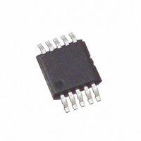
ISL95311UIU10Z-TK Intersil, ISL95311UIU10Z-TK Datasheet - Page 8

ISL95311UIU10Z-TK
Manufacturer Part Number
ISL95311UIU10Z-TK
Description
IC XDCP 128-TAP 50KOHM 10-MSOP
Manufacturer
Intersil
Series
XDCP™r
Datasheet
1.ISL95311WIU10Z-TK.pdf
(11 pages)
Specifications of ISL95311UIU10Z-TK
Taps
128
Resistance (ohms)
50K
Number Of Circuits
1
Temperature Coefficient
45 ppm/°C Typical
Memory Type
Non-Volatile
Interface
I²C, 2-Wire Serial
Voltage - Supply
2.7 V ~ 5.5 V
Operating Temperature
-40°C ~ 85°C
Mounting Type
Surface Mount
Package / Case
10-MSOP, Micro10™, 10-uMAX, 10-uSOP
Resistance In Ohms
50K
Lead Free Status / RoHS Status
Lead free / RoHS Compliant
SCL is HIGH. The ISL95311 continuously monitors the SDA
and SCL lines for the START condition and does not
respond to any command until this condition is met (see
Figure 1). A START condition is ignored during the power-up
sequence and during internal non-volatile write cycles.
All I
condition, which is a LOW to HIGH transition of SDA while
SCL is HIGH (see Figure 1). A STOP condition at the end of
a read operation, or at the end of a write operation to volatile
bytes only places the device in its standby mode. A STOP
condition during a write operation to a non-volatile byte,
initiates an internal non-volatile write cycle. The device
enters its standby state when the internal non-volatile write
cycle is completed.
An ACK, Acknowledge, is a software convention used to
indicate a successful data transfer. The transmitting device,
either master or slave, releases the SDA bus after
transmitting eight bits. During the ninth clock cycle, the
receiver pulls the SDA line LOW to acknowledge the
reception of the eight bits of data (see Figure 2).
The ISL95311 responds with an ACK after recognition of a
START condition followed by a valid Identification Byte, and
once again after successful receipt of an Address Byte. The
ISL95311 also responds with an ACK after receiving a Data
Byte of a write operation. The master must respond with an
ACK after receiving a Data Byte of a read operation
A valid Identification Byte contains 01010 as the five MSBs,
and the following two bits matching the logic values present
at pins A1, and A0. The LSB is in the Read/Write bit. Its
value is “1” for a Read operation, and “0” for a Write
operation (see Table 2.)
Write Operation
A Write operation requires a START condition, followed by a
valid Identification Byte, a valid Address Byte, a Data Byte, and
a STOP condition (see Figure 3). After each of the three bytes,
the ISL95311 responds with an ACK. At this time, if the Data
Byte is to be written only to volatile registers, then the device
enters its standby state. If the Data Byte is to be written also to
non-volatile memory, the ISL95311 begins its internal write
cycle to non-volatile memory. During the internal non-volatile
write cycle, the device ignores transitions at the SDA and SCL
pins, and the SDA output is at a high impedance state. When
the internal non-volatile write cycle is completed, the ISL95311
enters its standby state.
(MSB)
0
2
C interface operations must be terminated by a STOP
LOGIC VALUES AT PINS A1, AND A0 RESPECTIVELY
TABLE 2. DENTIFICATION BYTE FORMAT
1
0
1
8
0
A1
A0
(LSB)
R/W
ISL95311
The byte at address 02h determines if the Data Byte is to be
written to volatile and/or non-volatile memory (see “Memory
Description” on page 7).
Data Protection
A STOP condition also acts as a protection of non-volatile
memory. A valid Identification Byte, Address Byte, and total
number of SCL pulses act as a protection of both volatile
and non-volatile registers. During a Write sequence, the
Data Byte is loaded into an internal shift register as it is
received. If the Address Byte is 0 or 2, the Data Byte is
transferred to the Wiper Register (WR) or to the Access
Control Register respectively, at the falling edge of the SCL
pulse that loads the last bit (LSB) of the Data Byte. If the
Address Byte is 0, and the Access Control Register is all
zeros (default), then the STOP condition initiates the internal
write cycle to non-volatile memory.
Read Operation
A Read operation consists of a three byte instruction
followed by one or more Data Bytes (See Figure 4). The
master initiates the operation issuing the following
sequence: a START, the Identification byte with the R/W bit
set to “0”, an Address Byte, a second START, and a second
Identification byte with the R/W bit set to “1”. After each of
the three bytes, the ISL95311 responds with an ACK; then
the ISL95311 transmits the Data Byte. The master then
terminates the read operation (issuing a STOP condition)
following the last bit of the Data Byte (See Figure 4).
The byte at address 02h determines if the Data Bytes being
read are from volatile or non-volatile memory. (see “Memory
Description” on page 7.)
February 6, 2008
FN8084.1


