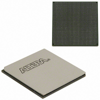
EP1AGX90EF1152C6 Altera, EP1AGX90EF1152C6 Datasheet - Page 108

EP1AGX90EF1152C6
Manufacturer Part Number
EP1AGX90EF1152C6
Description
IC ARRIA GX FPGA 90K 1152FBGA
Manufacturer
Altera
Series
Arria GXr
Datasheet
1.EP1AGX20CF484C6N.pdf
(234 pages)
Specifications of EP1AGX90EF1152C6
Number Of Logic Elements/cells
90220
Number Of Labs/clbs
4511
Total Ram Bits
4477824
Number Of I /o
538
Voltage - Supply
1.15 V ~ 1.25 V
Mounting Type
Surface Mount
Operating Temperature
0°C ~ 85°C
Package / Case
1152-FBGA
Lead Free Status / RoHS Status
Contains lead / RoHS non-compliant
Number Of Gates
-
Available stocks
Company
Part Number
Manufacturer
Quantity
Price
Company:
Part Number:
EP1AGX90EF1152C6
Manufacturer:
ALTERA
Quantity:
3 000
Company:
Part Number:
EP1AGX90EF1152C6N
Manufacturer:
ALTERA
Quantity:
3 000
2–102
Table 2–34. EP1AGX90 Device Differential Channels
Dedicated Circuitry with DPA Support
Figure 2–79. Arria GX Transmitter Channel
Arria GX Device Handbook, Volume 1
1,152-pin FineLine
BGA
Note to
(1) The total number of receiver channels includes the four non-dedicated clock channels that can be optionally used as data channels.
Package
Table
2–34:
refclk
Arria GX devices support source-synchronous interfacing with LVDS signaling at up
to 840 Mbps. Arria GX devices can transmit or receive serial channels along with a
low-speed or high-speed clock.
The receiving device PLL multiplies the clock by an integer factor W = 1 through 32.
The SERDES factor J determines the parallel data width to deserialize from receivers
or to serialize for transmitters. The SERDES factor J can be set to 4, 5, 6, 7, 8, 9, or 10
and does not have to equal the PLL clock-multiplication W value. A design using the
dynamic phase aligner also supports all of these J factor values. For a J factor of 1, the
Arria GX device bypasses the SERDES block. For a J factor of 2, the Arria GX device
bypasses the SERDES block, and the DDR input and output registers are used in the
IOE.
Each Arria GX receiver channel features a DPA block for phase detection and
selection, a SERDES, a synchronizer, and a data realigner circuit. You can bypass the
dynamic phase aligner without affecting the basic source-synchronous operation of
the channel. In addition, you can dynamically switch between using the DPA block or
bypassing the block via a control signal from the logic array.
Transmitter
Receiver
Transmitter/Receiver
Figure 2–79
Fast
PLL
Data from R4, R24, C4, or
direct link interconnect
Interconnect
Local
shows the block diagram of the Arria GX transmitter channel.
diffioclk
load_en
10
Total Channels
(Note 1)
10
45
47
PLL1
23
22
23
24
Center Fast PLLs
Dedicated
Transmitter
Interface
+
–
High-Speed Differential I/O with DPA Support
Regional or
global clock
Up to 840 Mbps
© December 2009 Altera Corporation
PLL2
22
23
24
23
Chapter 2: Arria GX Architecture
Corner Fast
PLL7
PLLs
23
—
23
—


