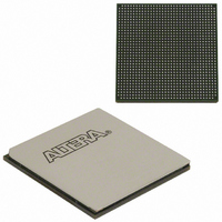
EP1AGX90EF1152C6 Altera, EP1AGX90EF1152C6 Datasheet - Page 96

EP1AGX90EF1152C6
Manufacturer Part Number
EP1AGX90EF1152C6
Description
IC ARRIA GX FPGA 90K 1152FBGA
Manufacturer
Altera
Series
Arria GXr
Datasheet
1.EP1AGX20CF484C6N.pdf
(234 pages)
Specifications of EP1AGX90EF1152C6
Number Of Logic Elements/cells
90220
Number Of Labs/clbs
4511
Total Ram Bits
4477824
Number Of I /o
538
Voltage - Supply
1.15 V ~ 1.25 V
Mounting Type
Surface Mount
Operating Temperature
0°C ~ 85°C
Package / Case
1152-FBGA
Lead Free Status / RoHS Status
Contains lead / RoHS non-compliant
Number Of Gates
-
Available stocks
Company
Part Number
Manufacturer
Quantity
Price
Company:
Part Number:
EP1AGX90EF1152C6
Manufacturer:
ALTERA
Quantity:
3 000
Company:
Part Number:
EP1AGX90EF1152C6N
Manufacturer:
ALTERA
Quantity:
3 000
2–90
Figure 2–76. Output Timing Diagram in DDR Mode
External RAM Interfacing
Table 2–23. DQS and DQ Bus Mode Support
Arria GX Device Handbook, Volume 1
EP1AGX20
EP1AGX35
EP1AGX50/60
EP1AGX90
Note to
(1) Numbers are preliminary until devices are available.
Device
Table
2–23:
484-pin FineLine BGA
484-pin FineLine BGA
780-pin FineLine BGA
484-pin FineLine BGA
780-pin FineLine BGA
1,152-pin FineLine
BGA
1,152-pin FineLine
BGA
From Internal
Registers
The Arria GX IOE operates in bidirectional DDR mode by combining the DDR input
and DDR output configurations. The negative-edge-clocked OE register holds the OE
signal inactive until the falling edge of the clock to meet DDR SDRAM timing
requirements.
In addition to the six I/O registers in each IOE, Arria GX devices also have dedicated
phase-shift circuitry for interfacing with external memory interfaces, including DDR,
DDR2 SDRAM, and SDR SDRAM. In every Arria GX device, the I/O banks at the top
(Banks 3 and 4) and bottom (Banks 7 and 8) of the device support DQ and DQS signals
with DQ bus modes of ×4, ×8/×9, ×16/×18, or ×32/×36.
of DQ and DQS buses that are supported per device.
A compensated delay element on each DQS pin automatically aligns input DQS
synchronization signals with the data window of their corresponding DQ data
signals. The DQS signals drive a local DQS bus in the top and bottom I/O banks. This
DQS bus is an additional resource to the I/O clocks and is used to clock DQ input
registers with the DQS signal.
DDR output
Package
CLK
A1
B1
B1
(Note 1)
Number of
×4 Groups
A1
18
18
36
36
2
2
2
B2
A2
B2
A2
A3
B3
B3
×8/×9 Groups
Number of
A3
18
18
A4
B4
0
0
8
0
8
B4
A4
×16/×18 Groups
Number of
Table 2–23
© December 2009 Altera Corporation
0
0
4
0
4
8
8
Chapter 2: Arria GX Architecture
shows the number
×32/×36 Groups
Number of
0
0
0
0
0
4
4
I/O Structure


