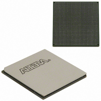
EP1AGX90EF1152C6 Altera, EP1AGX90EF1152C6 Datasheet - Page 147

EP1AGX90EF1152C6
Manufacturer Part Number
EP1AGX90EF1152C6
Description
IC ARRIA GX FPGA 90K 1152FBGA
Manufacturer
Altera
Series
Arria GXr
Datasheet
1.EP1AGX20CF484C6N.pdf
(234 pages)
Specifications of EP1AGX90EF1152C6
Number Of Logic Elements/cells
90220
Number Of Labs/clbs
4511
Total Ram Bits
4477824
Number Of I /o
538
Voltage - Supply
1.15 V ~ 1.25 V
Mounting Type
Surface Mount
Operating Temperature
0°C ~ 85°C
Package / Case
1152-FBGA
Lead Free Status / RoHS Status
Contains lead / RoHS non-compliant
Number Of Gates
-
Available stocks
Company
Part Number
Manufacturer
Quantity
Price
Company:
Part Number:
EP1AGX90EF1152C6
Manufacturer:
ALTERA
Quantity:
3 000
Company:
Part Number:
EP1AGX90EF1152C6N
Manufacturer:
ALTERA
Quantity:
3 000
Chapter 4: DC and Switching Characteristics
Power Consumption
Table 4–41. Series On-Chip Termination Specification for Left I/O Banks
Pin Capacitance
Table 4–42. Arria GX Device Capacitance
Power Consumption
© December 2009 Altera Corporation
25- R
50- R
3.3/2.5/1.8
50- R
R
C
C
C
C
C
C
Note to
(1) Capacitance is sample-tested only. Capacitance is measured using time-domain reflections (TDR). Measurement accuracy is within ±0.5 pF.
IOTB
IOL
CLKTB
CLKL
CLKL+
OUTFB
D
Symbol
Symbol
Table
S
S
S
3.3/2.5
1.5
4–42:
Input capacitance on I/O pins in I/O banks 3, 4, 7, and 8.
Input capacitance on I/O pins in I/O banks 1 and 2, including high-speed differential
receiver and transmitter pins.
Input capacitance on top/bottom clock input pins:
Input capacitance on left clock inputs:
Input capacitance on left clock inputs:
Input capacitance on dual-purpose clock output/feedback pins in PLL banks 11 and 12.
Internal series termination without
calibration (25- setting
Internal series termination without
calibration (50- setting
Internal series termination without
calibration (50- setting
Internal differential termination for
LVDS (100- setting)
Table 4–42
Altera offers two ways to calculate power for a design: the Excel-based PowerPlay
early power estimator power calculator and the Quartus II PowerPlay power analyzer
feature.
The interactive Excel-based PowerPlay Early Power Estimator is typically used prior
to designing the FPGA in order to get an estimate of device power. The Quartus II
PowerPlay Power Analyzer provides better quality estimates based on the specifics of
the design after place-and-route is complete. The power analyzer can apply a
combination of user-entered, simulation-derived and estimated signal activities
which, combined with detailed circuit models, can yield very accurate power
estimates.
In both cases, these calculations should only be used as an estimation of power, not as
a specification.
Description
shows the Arria GX device family pin capacitance.
(Note 1)
Parameter
CLK0
CLK1
and
and
V
CCIO
V
CCIO
CLK2
CLK3
V
V
Conditions
CLK[4..7]
= 3.3/2.5/1.8V
CCIO
CCIO
= 3.3/2.5V
.
.
= 1.5V
= 2.5V
and
CLK[12..15]
Commercial
Max
±30
±30
±36
±20
Resistance Tolerance
Arria GX Device Handbook, Volume 1
.
Industrial
Max
±30
±30
±36
±25
Typical
5.0
6.1
6.0
6.1
3.3
6.7
Units
Units
%
%
%
%
pF
pF
pF
pF
pF
pF
4–25


