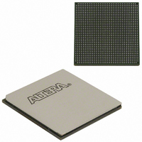
EP1AGX90EF1152C6 Altera, EP1AGX90EF1152C6 Datasheet - Page 124

EP1AGX90EF1152C6
Manufacturer Part Number
EP1AGX90EF1152C6
Description
IC ARRIA GX FPGA 90K 1152FBGA
Manufacturer
Altera
Series
Arria GXr
Datasheet
1.EP1AGX20CF484C6N.pdf
(234 pages)
Specifications of EP1AGX90EF1152C6
Number Of Logic Elements/cells
90220
Number Of Labs/clbs
4511
Total Ram Bits
4477824
Number Of I /o
538
Voltage - Supply
1.15 V ~ 1.25 V
Mounting Type
Surface Mount
Operating Temperature
0°C ~ 85°C
Package / Case
1152-FBGA
Lead Free Status / RoHS Status
Contains lead / RoHS non-compliant
Number Of Gates
-
Available stocks
Company
Part Number
Manufacturer
Quantity
Price
Company:
Part Number:
EP1AGX90EF1152C6
Manufacturer:
ALTERA
Quantity:
3 000
Company:
Part Number:
EP1AGX90EF1152C6N
Manufacturer:
ALTERA
Quantity:
3 000
4–2
Table 4–1. Arria GX Device Absolute Maximum Ratings
Recommended Operating Conditions
Table 4–3. Arria GX Device Recommended Operating Conditions (Part 1 of 2)
Arria GX Device Handbook, Volume 1
T
Notes to
(1) For more information about operating requirements for Altera
(2) Conditions beyond those listed in
(3) Supply voltage specifications apply to voltage readings taken at the device pins, not at the power supply.
(4) During transitions, the inputs may overshoot to the voltage shown in
V
V
V
V
V
J
CCINT
CCIO
CCPD
I
O
Symbol
ratings for extended periods of time may have adverse affects on the device.
100% duty cycle. During transitions, the inputs may undershoot to –2.0 V for input currents less than 100 mA and periods shorter than 20 ns.
Symbol
Table
4–1:
Supply voltage for internal
logic and input buffers
Supply voltage for output
buffers, 3.3-V operation
Supply voltage for output
buffers, 2.5-V operation
Supply voltage for output
buffers, 1.8-V operation
Supply voltage for output
buffers, 1.5-V operation
Supply voltage for output
buffers, 1.2-V operation
Supply voltage for pre-drivers
as well as configuration and
JTAG I/O buffers.
Input voltage
(refer to
Output voltage
Junction temperature
Table 4–2. Maximum Duty Cycles in Voltage Transitions
Table 4–3
Note to
(1) During transition, the inputs may overshoot to the voltages shown based on the input duty cycle. The DC case is
Table
Parameter
equivalent to 100% duty cycle.
Parameter
Symbol
Table
4–2)
Table 4–1
V
I
lists the recommended operating conditions for the Arria GX device family.
4–2:
may cause permanent damage to a device. Additionally, device operation at the absolute maximum
Maximum duty cycles in
voltage transitions
BGA packages under bias
Rise time 100 ms
Rise time 100 ms (3),
Rise time 100 ms
Rise time 100 ms
Rise time 100 ms
Rise time 100 ms
100 s rise time 100 ms
(2),
Parameter
(5)
®
devices, refer to the
Conditions
(Note
Table 4–2
Conditions
—
1), (2),
based upon the input duty cycle. The DC case is equivalent to
(3)
(3)
(3)
(3)
(3)
Arria GX Device Family Data Sheet
(6)
(3)
Condition
V
V
V
V
V
V
I
I
I
I
I
I
= 4.0 V
= 4.2 V
= 4.3 V
= 4.4 V
= 4.5 V
= 4.1 V
(Part 2 of 2)
(4)
Minimum
(Note 1)
–55
Chapter 4: DC and Switching Characteristics
(Note 1)
Minimum
(3.00)
3.135
2.375
1.425
3.135
© December 2009 Altera Corporation
1.15
1.71
1.15
–0.5
0
(Part 1 of 2)
Maximum Duty Cycles (%)
Maximum
125
Maximum
(3.60)
chapter.
3.465
2.625
1.575
3.465
V
100
1.25
1.89
1.25
4.0
Operating Conditions
90
50
30
17
10
CCIO
Units
C
Units
V
V
V
V
V
V
V
V
V


