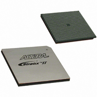
EP2SGX90FF1508C3N Altera, EP2SGX90FF1508C3N Datasheet - Page 299

EP2SGX90FF1508C3N
Manufacturer Part Number
EP2SGX90FF1508C3N
Description
IC STRATIX II GX 90K 1508-FBGA
Manufacturer
Altera
Series
Stratix® II GXr
Datasheet
1.EP2SGX90FF1508C3N.pdf
(314 pages)
Specifications of EP2SGX90FF1508C3N
Number Of Logic Elements/cells
90960
Number Of Labs/clbs
4548
Total Ram Bits
4520448
Number Of I /o
650
Voltage - Supply
1.15 V ~ 1.25 V
Mounting Type
Surface Mount
Operating Temperature
0°C ~ 70°C
Package / Case
1508-FBGA
For Use With
544-1725 - PCIE KIT W/S II GX EP2SGX90N544-1724 - SI KIT W/SII GX EP2SGX90N544-1702 - VIDEO KIT W/SII GX EP2SGX90N
Lead Free Status / RoHS Status
Lead free / RoHS Compliant
Number Of Gates
-
Other names
544-1772
EP2SGX90FF40C3N
EP2SGX90FF40C3NES
EP2SGX90FF40C3N
EP2SGX90FF40C3NES
Available stocks
Company
Part Number
Manufacturer
Quantity
Price
Company:
Part Number:
EP2SGX90FF1508C3N
Manufacturer:
ALTERA30
Quantity:
121
- Current page: 299 of 314
- Download datasheet (4Mb)
Altera Corporation
October 2007
Notes to
(1)
(2)
(3)
(4)
f
f
f
TCCS
SW
Output jitter
Output t
Output t
t
DPA run length
DPA jitter tolerance
DPA lock time
I N
H S D R
H S D R D PA
DUTY
Table 4–109. High-Speed I/O Specifications for -5 Speed Grade
= f
When J = 4 to 10, the SERDES block is used.
When J = 1 or 2, the SERDES block is bypassed.
The input clock frequency and the W factor must satisfy the following fast PLL VCO specification: 150 ≤ input clock
frequency × W ≤ 840.
The minimum specification is dependent on the clock source (fast PLL, enhanced PLL, clock pin, and so on) and
the clock routing resource (global, regional, or local) utilized. The I/O differential buffer and input register do not
have a minimum toggle rate.
H S D R
(data rate)
R I S E
FA L L
Table
Symbol
(DPA data rate) J = 4 to 10 (LVDS, HyperTransport technology)
/ W
4–109:
W = 2 to 32 (LVDS, HyperTransport technology)
(3)
W = 1 (SERDES bypass, LVDS only)
W = 1 (SERDES used, LVDS only)
J = 4 to 10 (LVDS, HyperTransport technology)
J = 2 (LVDS, HyperTransport technology)
J = 1 (LVDS only)
All differential I/O standards
All differential I/O standards
All differential I/O standards
All differential I/O standards
Data channel peak-to-peak jitter
SPI-4
Parallel Rapid I/O
Miscellaneous
Table 4–109
grade Stratix II GX devices.
Standard
shows the high-speed I/O timing specifications for -5 speed
Conditions
0000000000
1111111111
00001111
10010000
10101010
01010101
Training
Pattern
Transition
Density
100%
10%
25%
50%
Stratix II GX Device Handbook, Volume 1
Notes
DC and Switching Characteristics
0.44
Min
150
150
256
256
256
256
256
150
440
(1),
16
16
(4)
(4)
45
-5 Speed Grade
-
(2)
Typ
50
6,400
Max
420
500
640
840
700
500
840
200
190
290
290
55
-
Number of
repetitions
Mbps
Mbps
Mbps
Mbps
MHz
MHz
MHz
Unit
ps
ps
ps
ps
ps
UI
UI
%
4–129
Related parts for EP2SGX90FF1508C3N
Image
Part Number
Description
Manufacturer
Datasheet
Request
R

Part Number:
Description:
CYCLONE II STARTER KIT EP2C20N
Manufacturer:
Altera
Datasheet:

Part Number:
Description:
CPLD, EP610 Family, ECMOS Process, 300 Gates, 16 Macro Cells, 16 Reg., 16 User I/Os, 5V Supply, 35 Speed Grade, 24DIP
Manufacturer:
Altera Corporation
Datasheet:

Part Number:
Description:
CPLD, EP610 Family, ECMOS Process, 300 Gates, 16 Macro Cells, 16 Reg., 16 User I/Os, 5V Supply, 15 Speed Grade, 24DIP
Manufacturer:
Altera Corporation
Datasheet:

Part Number:
Description:
Manufacturer:
Altera Corporation
Datasheet:

Part Number:
Description:
CPLD, EP610 Family, ECMOS Process, 300 Gates, 16 Macro Cells, 16 Reg., 16 User I/Os, 5V Supply, 30 Speed Grade, 24DIP
Manufacturer:
Altera Corporation
Datasheet:

Part Number:
Description:
High-performance, low-power erasable programmable logic devices with 8 macrocells, 10ns
Manufacturer:
Altera Corporation
Datasheet:

Part Number:
Description:
High-performance, low-power erasable programmable logic devices with 8 macrocells, 7ns
Manufacturer:
Altera Corporation
Datasheet:

Part Number:
Description:
Classic EPLD
Manufacturer:
Altera Corporation
Datasheet:

Part Number:
Description:
High-performance, low-power erasable programmable logic devices with 8 macrocells, 10ns
Manufacturer:
Altera Corporation
Datasheet:

Part Number:
Description:
Manufacturer:
Altera Corporation
Datasheet:

Part Number:
Description:
Manufacturer:
Altera Corporation
Datasheet:

Part Number:
Description:
Manufacturer:
Altera Corporation
Datasheet:

Part Number:
Description:
CPLD, EP610 Family, ECMOS Process, 300 Gates, 16 Macro Cells, 16 Reg., 16 User I/Os, 5V Supply, 25 Speed Grade, 24DIP
Manufacturer:
Altera Corporation
Datasheet:


